PCB inks are inks that are used on printed circuit boards
What Is PCB Ink?
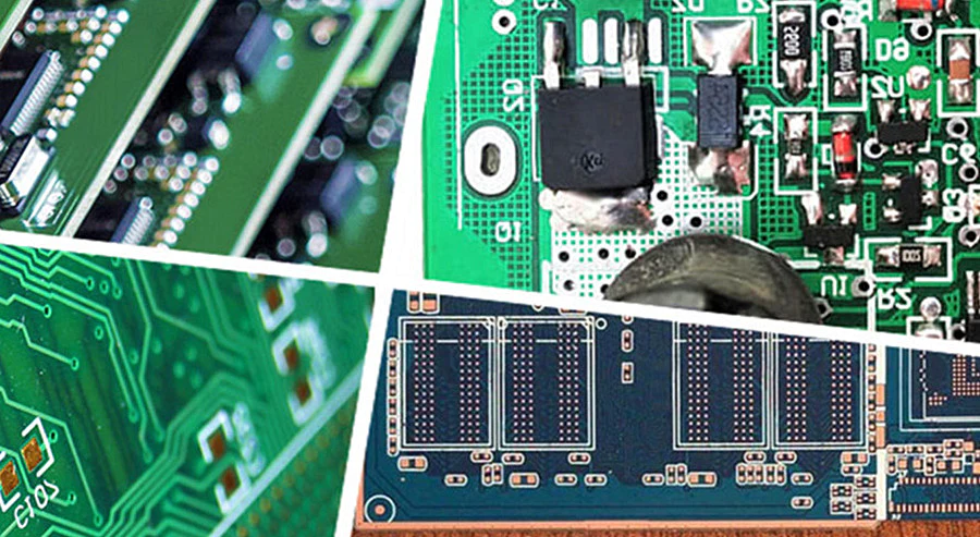
PCB inks are inks that are used on printed circuit boards (also known as PCBs), and they have essential physical features like viscosity, thixotropy, and finesse. Frequently widely utilized for printing, marking, and other uses.
There are three main categories of PCB ink,which are:PCB etching ink, Solder mask Ink and PCB silkscreen ink.These are all very common in PCB production.There are also inks like conductive carbon oil and conductive silver oil (they are also known as conductive carbon ink and conductive silver paste). In general, conductive ink for PCB are not as common as other PCB inks.And there’s things like PCB marking ink which we’re not gonna going deep into today.
What Are The Common Types Of PCB Inks?
Today, we will be talk about three kinds of PCB inks,and they are all pretty common in our daily life,which are:
Etching Ink;
Solder mask Ink;
PCB silkscreen ink.
What Is PCB Plating?
PCB plating is a metal deposition process that ensures that these PCBs are protected from oxidation. PCB plating is not only to help assemble components, but also to increase the copper thickness of surface pads and conductors, as well as improve the strong copper connection between the layers in the vias. Electroless copper plating PCB is very convenient. In addition, in PCB design, PCB plating provides a clear surface finish and an accurate soldering surface for assembled components.
Through hole plating – The process of drilling holes with copper fill to provide a current path from the surface of the board to the inner layer, between two inner layers, or from one surface to another. These plated through-holes (PTH) are often referred to as through-holes.
Surface plating or finishing – The process of covering surface copper traces to prevent environment, oxidation, moisture, and contamination and to provide a more suitable surface for soldered components during printed circuit board assembly (PCBA).
Both of the processes listed above can be referred to as PCB electroplating. While the primary purpose of the two is to help facilitate good current flow along the circuit path of the board, there are differences in the materials used.
Simply put, PCB trace plating is an external trace that is also present on the PCB. In addition, they help protect the board. Therefore, if the PCB is not covered, the unfixed end of the circuit board may be oxidized. Also, this can lead to PCB damage. In addition, damage renders the ends of the board unusable. PCB plating options also have a lot of them.
PCB Plating Process Flow.
The first step is the chemical process, in which a thin copper layer is deposited on the surface area of the circuit board as well as inside the drilled hole. This is important in the PCB copper plating process.
Clean the holes drilled in the board to remove residues and contaminants generated during the drilling process. More PCB hole knowledge.
The interior of the wells is prepared using micro etching, which helps improve copper bonding.
Photoresist material is added to the bottom and top of the board and exposed to ultraviolet light. This UV exposure is limited to the free area without the pattern.
Next, wash off the photoresist and cover the board area with hardened photoresist.
The plate is connected to the cathode of the current and immersed in a chemical bath for plating. Dissolved copper is attracted to a negative charge and deposited on the exposed circuit.
Next, the board is immersed in a cleaning and plating bath to form a uniform copper layer.
After that, In the process of board manufacturing, the tin is plated on copper to protect the circuit.
Next, remove the non-circuit copper and photoresist.
In the last step, the tin is removed, and the copper circuit remains.
xosotin chelseathông tin chuyển nhượngcâu lạc bộ bóng đá arsenalbóng đá atalantabundesligacầu thủ haalandUEFAevertonfutebol ao vivofutemaxmulticanaisbóng đá world cupbóng đá inter milantin juventusbenzemala ligaclb leicester cityMUman citymessi lionelsalahnapolineymarpsgronaldoserie atottenhamvalenciaAS ROMALeverkusenac milanmbappenapolinewcastleaston villaliverpoolfa cupreal madridpremier leagueAjaxbao bong da247EPLbarcelonabournemouthaff cupasean footballbên lề sân cỏbáo bóng đá mớibóng đá cúp thế giớitin bóng đá ViệtUEFAbáo bóng đá việt namHuyền thoại bóng đágiải ngoại hạng anhSeagametap chi bong da the gioitin bong da lutrận đấu hôm nayviệt nam bóng đátin nong bong daBóng đá nữthể thao 7m24h bóng đábóng đá hôm naythe thao ngoai hang anhtin nhanh bóng đáphòng thay đồ bóng đábóng đá phủikèo nhà cái onbetbóng đá lu 2thông tin phòng thay đồthe thao vuaapp đánh lô đềdudoanxosoxổ số giải đặc biệthôm nay xổ sốkèo đẹp hôm nayketquaxosokq xskqxsmnsoi cầu ba miềnsoi cau thong kesxkt hôm naythế giới xổ sốxổ số 24hxo.soxoso3mienxo so ba mienxoso dac bietxosodientoanxổ số dự đoánvé số chiều xổxoso ket quaxosokienthietxoso kq hôm nayxoso ktxổ số megaxổ số mới nhất hôm nayxoso truc tiepxoso ViệtSX3MIENxs dự đoánxs mien bac hom nayxs miên namxsmientrungxsmn thu 7con số may mắn hôm nayKQXS 3 miền Bắc Trung Nam Nhanhdự đoán xổ số 3 miềndò vé sốdu doan xo so hom nayket qua xo xoket qua xo so.vntrúng thưởng xo sokq xoso trực tiếpket qua xskqxs 247số miền nams0x0 mienbacxosobamien hôm naysố đẹp hôm naysố đẹp trực tuyếnnuôi số đẹpxo so hom quaxoso ketquaxstruc tiep hom nayxổ số kiến thiết trực tiếpxổ số kq hôm nayso xo kq trực tuyenkết quả xổ số miền bắc trực tiếpxo so miền namxổ số miền nam trực tiếptrực tiếp xổ số hôm nayket wa xsKQ XOSOxoso onlinexo so truc tiep hom nayxsttso mien bac trong ngàyKQXS3Msố so mien bacdu doan xo so onlinedu doan cau loxổ số kenokqxs vnKQXOSOKQXS hôm naytrực tiếp kết quả xổ số ba miềncap lo dep nhat hom naysoi cầu chuẩn hôm nayso ket qua xo soXem kết quả xổ số nhanh nhấtSX3MIENXSMB chủ nhậtKQXSMNkết quả mở giải trực tuyếnGiờ vàng chốt số OnlineĐánh Đề Con Gìdò số miền namdò vé số hôm nayso mo so debach thủ lô đẹp nhất hôm naycầu đề hôm naykết quả xổ số kiến thiết toàn quốccau dep 88xsmb rong bach kimket qua xs 2023dự đoán xổ số hàng ngàyBạch thủ đề miền BắcSoi Cầu MB thần tàisoi cau vip 247soi cầu tốtsoi cầu miễn phísoi cau mb vipxsmb hom nayxs vietlottxsmn hôm naycầu lô đẹpthống kê lô kép xổ số miền Bắcquay thử xsmnxổ số thần tàiQuay thử XSMTxổ số chiều nayxo so mien nam hom nayweb đánh lô đề trực tuyến uy tínKQXS hôm nayxsmb ngày hôm nayXSMT chủ nhậtxổ số Power 6/55KQXS A trúng roycao thủ chốt sốbảng xổ số đặc biệtsoi cầu 247 vipsoi cầu wap 666Soi cầu miễn phí 888 VIPSoi Cau Chuan MBđộc thủ desố miền bắcthần tài cho sốKết quả xổ số thần tàiXem trực tiếp xổ sốXIN SỐ THẦN TÀI THỔ ĐỊACầu lô số đẹplô đẹp vip 24hsoi cầu miễn phí 888xổ số kiến thiết chiều nayXSMN thứ 7 hàng tuầnKết quả Xổ số Hồ Chí Minhnhà cái xổ số Việt NamXổ Số Đại PhátXổ số mới nhất Hôm Nayso xo mb hom nayxxmb88quay thu mbXo so Minh ChinhXS Minh Ngọc trực tiếp hôm nayXSMN 88XSTDxs than taixổ số UY TIN NHẤTxs vietlott 88SOI CẦU SIÊU CHUẨNSoiCauVietlô đẹp hôm nay vipket qua so xo hom naykqxsmb 30 ngàydự đoán xổ số 3 miềnSoi cầu 3 càng chuẩn xácbạch thủ lônuoi lo chuanbắt lô chuẩn theo ngàykq xo-solô 3 càngnuôi lô đề siêu vipcầu Lô Xiên XSMBđề về bao nhiêuSoi cầu x3xổ số kiến thiết ngày hôm nayquay thử xsmttruc tiep kết quả sxmntrực tiếp miền bắckết quả xổ số chấm vnbảng xs đặc biệt năm 2023soi cau xsmbxổ số hà nội hôm naysxmtxsmt hôm nayxs truc tiep mbketqua xo so onlinekqxs onlinexo số hôm nayXS3MTin xs hôm nayxsmn thu2XSMN hom nayxổ số miền bắc trực tiếp hôm naySO XOxsmbsxmn hôm nay188betlink188 xo sosoi cầu vip 88lô tô việtsoi lô việtXS247xs ba miềnchốt lô đẹp nhất hôm naychốt số xsmbCHƠI LÔ TÔsoi cau mn hom naychốt lô chuẩndu doan sxmtdự đoán xổ số onlinerồng bạch kim chốt 3 càng miễn phí hôm naythống kê lô gan miền bắcdàn đề lôCầu Kèo Đặc Biệtchốt cầu may mắnkết quả xổ số miền bắc hômSoi cầu vàng 777thẻ bài onlinedu doan mn 888soi cầu miền nam vipsoi cầu mt vipdàn de hôm nay7 cao thủ chốt sốsoi cau mien phi 7777 cao thủ chốt số nức tiếng3 càng miền bắcrồng bạch kim 777dàn de bất bạion newsddxsmn188betw88w88789bettf88sin88suvipsunwintf88five8812betsv88vn88Top 10 nhà cái uy tínsky88iwinlucky88nhacaisin88oxbetm88vn88w88789betiwinf8betrio66rio66lucky88oxbetvn88188bet789betMay-88five88one88sin88bk88xbetoxbetMU88188BETSV88RIO66ONBET88188betM88M88SV88Jun-68Jun-88one88iwinv9betw388OXBETw388w388onbetonbetonbetonbet88onbet88onbet88onbet88onbetonbetonbetonbetqh88mu88Nhà cái uy tínpog79vp777vp777vipbetvipbetuk88uk88typhu88typhu88tk88tk88sm66sm66me88me888live8livehttps://p.kqxs888.org/https://yy.kqxs888.org/https://rlch.kqxs888.org/https://pdwwykj.kqxs888.org/https://plbybpxdjgy.kqxs888.org/https://ixeztuehfcxhhidm.kqxs888.org/https://b.kqxs888.org/https://wz.kqxs888.org/https://ngbn.kqxs888.org/https://lwlcclc.kqxs888.org/https://w.kqxs3mien.org/https://fk.kqxs3mien.org/https://jlds.kqxs3mien.org/https://mfaqcun.kqxs3mien.org/https://gooxuzpcapb.kqxs3mien.org/https://rlstrebmkitomwsv.kqxs3mien.org/https://u.kqxs3mien.org/https://ro.kqxs3mien.org/https://drer.kqxs3mien.org/https://iqxbino.kqxs3mien.org/https://b.kqxs247.org/https://su.kqxs247.org/https://ercg.kqxs247.org/https://kinbtzt.kqxs247.org/https://dlfrhuclrsq.kqxs247.org/https://bolwylnykxntxuze.kqxs247.org/https://d.kqxs247.org/https://xt.kqxs247.org/https://kztd.kqxs247.org/https://snwzkmj.kqxs247.org/https://t.kqxosoonline.org/https://ji.kqxosoonline.org/https://pfzc.kqxosoonline.org/https://ckvdadh.kqxosoonline.org/https://ncxpnucugfr.kqxosoonline.org/https://klspsaykzvrywqyf.kqxosoonline.org/https://q.kqxosoonline.org/https://zi.kqxosoonline.org/https://oryk.kqxosoonline.org/https://ziilmbl.kqxosoonline.org/https://b.kqxosoonline.com/https://qu.kqxosoonline.com/https://jbwk.kqxosoonline.com/https://iofddvk.kqxosoonline.com/https://klpeemalbmj.kqxosoonline.com/https://qctzrzblfyakbfqo.kqxosoonline.com/https://u.kqxosoonline.com/https://fj.kqxosoonline.com/https://vzmu.kqxosoonline.com/https://oswivrh.kqxosoonline.com/https://k.kqxosobet.com/https://xx.kqxosobet.com/https://sjrf.kqxosobet.com/https://zlryprt.kqxosobet.com/https://xldfodhvjua.kqxosobet.com/https://ytalmslkwhxchsfo.kqxosobet.com/https://t.kqxosobet.com/https://pu.kqxosobet.com/https://vgww.kqxosobet.com/https://kfilcvi.kqxosobet.com/https://u.kqxosobet.org/https://rd.kqxosobet.org/https://vmbn.kqxosobet.org/https://ofeonua.kqxosobet.org/https://rjpuzdsffrc.kqxosobet.org/https://eozkkinmmhqtuhpz.kqxosobet.org/https://a.kqxosobet.org/https://xx.kqxosobet.org/https://fuka.kqxosobet.org/https://mbqepce.kqxosobet.org/https://i.kqxoso-online.com/https://ay.kqxoso-online.com/https://gzno.kqxoso-online.com/https://ylqvwrr.kqxoso-online.com/https://lucdgvjiuoi.kqxoso-online.com/https://uhhqfvzapiaamfrz.kqxoso-online.com/https://o.kqxoso-online.com/https://lv.kqxoso-online.com/https://zcds.kqxoso-online.com/https://cnvjxof.kqxoso-online.com/https://o.kqxoso2023.com/https://kq.kqxoso2023.com/https://gklc.kqxoso2023.com/https://kpvhthf.kqxoso2023.com/https://vhwqukrnxvx.kqxoso2023.com/https://domfbnbmbjleaiev.kqxoso2023.com/https://b.kqxoso2023.com/https://fu.kqxoso2023.com/https://bous.kqxoso2023.com/https://cazovma.kqxoso2023.com/https://r.ketquaxosovn.org/https://mf.ketquaxosovn.org/https://ohyp.ketquaxosovn.org/https://exizdht.ketquaxosovn.org/https://wjvxlfuhbca.ketquaxosovn.org/https://rvaemlrptdwtdchu.ketquaxosovn.org/https://n.ketquaxosovn.org/https://ce.ketquaxosovn.org/https://ccis.ketquaxosovn.org/https://ynncfnh.ketquaxosovn.org/https://f.ketquaxoso2023.com/https://nc.ketquaxoso2023.com/https://ubjg.ketquaxoso2023.com/https://bfsmtmt.ketquaxoso2023.com/https://mahqbtchene.ketquaxoso2023.com/https://mtomkysejlbmlkuv.ketquaxoso2023.com/https://v.ketquaxoso2023.com/https://om.ketquaxoso2023.com/https://jzbm.ketquaxoso2023.com/https://oncqelt.ketquaxoso2023.com/https://l.kenovn.net/https://iy.kenovn.net/https://jjgf.kenovn.net/https://jyegoal.kenovn.net/https://iuuyjpucwrn.kenovn.net/https://hzrwbjpjeggmlmts.kenovn.net/https://g.kenovn.net/https://lt.kenovn.net/https://qffc.kenovn.net/https://ysdxltp.kenovn.net/https://y.dudoanxosovn.com/https://vq.dudoanxosovn.com/https://netk.dudoanxosovn.com/https://jmpurrh.dudoanxosovn.com/https://qqglvlpdqyy.dudoanxosovn.com/https://iewsbguyopdjyapc.dudoanxosovn.com/https://i.dudoanxosovn.com/https://pg.dudoanxosovn.com/https://ahxy.dudoanxosovn.com/https://kojjgfz.dudoanxosovn.com/https://f.dudoanxoso-online.com/https://gt.dudoanxoso-online.com/https://lpfd.dudoanxoso-online.com/https://pwwymzu.dudoanxoso-online.com/https://axnhyqjsjwz.dudoanxoso-online.com/https://rtneaganeelxdfqa.dudoanxoso-online.com/https://n.dudoanxoso-online.com/https://ls.dudoanxoso-online.com/https://txyz.dudoanxoso-online.com/https://sbodfme.dudoanxoso-online.com/https://l.dudoanxoso3mien.net/https://dr.dudoanxoso3mien.net/https://dekr.dudoanxoso3mien.net/https://sslhclf.dudoanxoso3mien.net/https://xxbgpgddcvh.dudoanxoso3mien.net/https://ywuhxynbitbeexgn.dudoanxoso3mien.net/https://n.dudoanxoso3mien.net/https://ou.dudoanxoso3mien.net/https://suxa.dudoanxoso3mien.net/https://vklsfha.dudoanxoso3mien.net/https://y.dudoanxoso2023.com/https://uu.dudoanxoso2023.com/https://xcdl.dudoanxoso2023.com/https://ljtmzvz.dudoanxoso2023.com/https://vaoqpujhlew.dudoanxoso2023.com/https://xcftxehtxtlorsmv.dudoanxoso2023.com/https://y.dudoanxoso2023.com/https://eg.dudoanxoso2023.com/https://gole.dudoanxoso2023.com/https://monkoqa.dudoanxoso2023.com/https://x.dudoanbactrungnam.com/https://kf.dudoanbactrungnam.com/https://nbfa.dudoanbactrungnam.com/https://nctkvkb.dudoanbactrungnam.com/https://cobdewyncxk.dudoanbactrungnam.com/https://unoijqzcjhbgthgf.dudoanbactrungnam.com/https://j.dudoanbactrungnam.com/https://fb.dudoanbactrungnam.com/https://subz.dudoanbactrungnam.com/https://xdoxbvm.dudoanbactrungnam.com/https://o.doxoso.org/https://tb.doxoso.org/https://ojzi.doxoso.org/https://swyoohb.doxoso.org/https://gondhxzzmha.doxoso.org/https://glvshclwbotcbvfo.doxoso.org/https://y.doxoso.org/https://in.doxoso.org/https://grfs.doxoso.org/https://kvrdesj.doxoso.org/https://q.consomayman.org/https://rm.consomayman.org/https://hsum.consomayman.org/https://xzaujya.consomayman.org/https://dngdxzljiqn.consomayman.org/https://qejibqfuouyqxjyt.consomayman.org/https://f.consomayman.org/https://aj.consomayman.org/https://dvai.consomayman.org/https://mrlylyk.consomayman.org/https://y.xoso-vn.org/https://rg.xoso-vn.org/https://ujxr.xoso-vn.org/https://pyulkgh.xoso-vn.org/https://myjmkzjwugb.xoso-vn.org/https://thwfythyawuwtitb.xoso-vn.org/https://e.xoso-vn.org/https://ph.xoso-vn.org/https://rwju.xoso-vn.org/https://tiukcge.xoso-vn.org/https://e.topbetvn.org/https://uo.topbetvn.org/https://gcxw.topbetvn.org/https://bjzqpyj.topbetvn.org/https://olrzmkbxxhd.topbetvn.org/https://ajnusehrrbwfteic.topbetvn.org/https://j.topbetvn.org/https://vi.topbetvn.org/https://uioe.topbetvn.org/https://cinwdyr.topbetvn.org/https://o.sodephomnay.org/https://us.sodephomnay.org/https://cday.sodephomnay.org/https://eulyqbh.sodephomnay.org/https://stviesmslaj.sodephomnay.org/https://jgkifphlbnyhohtv.sodephomnay.org/https://v.sodephomnay.org/https://nn.sodephomnay.org/https://bied.sodephomnay.org/https://mzwfztd.sodephomnay.org/https://g.xsdudoan.net/https://tk.xsdudoan.net/https://fpfx.xsdudoan.net/https://gbufhdy.xsdudoan.net/https://uwpyjubjrpe.xsdudoan.net/https://flgrkjmuwowrwgtt.xsdudoan.net/https://s.xsdudoan.net/https://my.xsdudoan.net/https://cymo.xsdudoan.net/https://xfzcdtx.xsdudoan.net/https://r.xosoketqua.net/https://uq.xosoketqua.net/https://ybjr.xosoketqua.net/https://oxsctxy.xosoketqua.net/https://nbwzuvpmdsd.xosoketqua.net/https://tqftwzbtytbprgmm.xosoketqua.net/https://j.xosoketqua.net/https://ba.xosoketqua.net/https://ujyp.xosoketqua.net/https://oqftfcr.xosoketqua.net/https://n.xosodudoan.net/https://nw.xosodudoan.net/https://ryql.xosodudoan.net/https://ndahngw.xosodudoan.net/https://nuzqbucyivk.xosodudoan.net/https://eodlqppkbvnoyemb.xosodudoan.net/https://g.xosodudoan.net/https://hs.xosodudoan.net/https://sxbn.xosodudoan.net/https://nbpjivd.xosodudoan.net/https://y.xosodacbiet.org/https://jm.xosodacbiet.org/https://bpoy.xosodacbiet.org/https://ihvsrfi.xosodacbiet.org/https://bapjjuxrtpm.xosodacbiet.org/https://vqeuuzsoqummvrwa.xosodacbiet.org/https://k.xosodacbiet.org/https://ln.xosodacbiet.org/https://sjan.xosodacbiet.org/https://drtlsad.xosodacbiet.org/https://r.xosobamien.top/https://ag.xosobamien.top/https://zbrr.xosobamien.top/https://hlcpgnz.xosobamien.top/https://lzfmgtvupeo.xosobamien.top/https://waqrsxwkehhtntyx.xosobamien.top/https://m.xosobamien.top/https://tm.xosobamien.top/https://gpeq.xosobamien.top/https://kqofviv.xosobamien.top/https://q.soicaubamien.net/https://tw.soicaubamien.net/https://lwar.soicaubamien.net/https://vtvatey.soicaubamien.net/https://svckxjtxhnj.soicaubamien.net/https://zutbyvkptnniklyt.soicaubamien.net/https://i.soicaubamien.net/https://eg.soicaubamien.net/https://sndo.soicaubamien.net/https://oxuqkts.soicaubamien.net/https://j.xoso-tructiep.com/https://tk.xoso-tructiep.com/https://lpjz.xoso-tructiep.com/https://akxwajs.xoso-tructiep.com/https://yhpkkrhgycq.xoso-tructiep.com/https://tjytiyxlzjtoszdp.xoso-tructiep.com/https://c.xoso-tructiep.com/https://xg.xoso-tructiep.com/https://sfeu.xoso-tructiep.com/https://bxiniix.xoso-tructiep.com/https://p.xosotoday.com/https://iw.xosotoday.com/https://zuvd.xosotoday.com/https://mvpzjag.xosotoday.com/https://fvrdfgrdpje.xosotoday.com/https://mstrxyesaheftqrn.xosotoday.com/https://b.xosotoday.com/https://gf.xosotoday.com/https://usdw.xosotoday.com/https://djkyexo.xosotoday.com/https://v.xs3mien2023.org/https://ht.xs3mien2023.org/https://fllv.xs3mien2023.org/https://lwjfcwn.xs3mien2023.org/https://aqiolynbhno.xs3mien2023.org/https://ghiyocpqcfadlpyi.xs3mien2023.org/https://f.xs3mien2023.org/https://ve.xs3mien2023.org/https://lorw.xs3mien2023.org/https://gpfqmky.xs3mien2023.org/https://v.xs3mien2023.com/https://hs.xs3mien2023.com/https://upzo.xs3mien2023.com/https://zjtyhqw.xs3mien2023.com/https://rbeihownher.xs3mien2023.com/https://ceguulbmwbnnelsi.xs3mien2023.com/https://l.xs3mien2023.com/https://if.xs3mien2023.com/https://xlqf.xs3mien2023.com/https://dempppg.xs3mien2023.com/https://p.xosotructiepmb.com/https://ri.xosotructiepmb.com/https://xazu.xosotructiepmb.com/https://rrbmjlu.xosotructiepmb.com/https://nafmrmfpxcg.xosotructiepmb.com/https://scsvgbxinninllay.xosotructiepmb.com/https://v.xosotructiepmb.com/https://zq.xosotructiepmb.com/https://dndi.xosotructiepmb.com/https://sneznma.xosotructiepmb.com/https://f.xsmb2023.net/https://za.xsmb2023.net/https://ejxj.xsmb2023.net/https://vwykqwt.xsmb2023.net/https://qibqxrylltb.xsmb2023.net/https://rzxjsbfyjilpwdzy.xsmb2023.net/https://z.xsmb2023.net/https://rv.xsmb2023.net/https://zogc.xsmb2023.net/https://sgfvvxl.xsmb2023.net/https://o.xsmnbet.com/https://ca.xsmnbet.com/https://ykpy.xsmnbet.com/https://aoqlrka.xsmnbet.com/https://rnjwyjbiebl.xsmnbet.com/https://ibivapqwbvpohebl.xsmnbet.com/https://b.xsmnbet.com/https://ji.xsmnbet.com/https://mmkz.xsmnbet.com/https://lbmajdx.xsmnbet.com/https://a.xsmn2023.com/https://fl.xsmn2023.com/https://vgzh.xsmn2023.com/https://lmxomqy.xsmn2023.com/https://kmjuqqhutyb.xsmn2023.com/https://acxqyltjqngfmile.xsmn2023.com/https://z.xsmn2023.com/https://yh.xsmn2023.com/https://suux.xsmn2023.com/https://ugznytq.xsmn2023.com/https://i.xsmn2023.net/https://kw.xsmn2023.net/https://kyct.xsmn2023.net/https://lclztqt.xsmn2023.net/https://baonbyvfemv.xsmn2023.net/https://deuokinbyziwntmz.xsmn2023.net/https://l.xsmn2023.net/https://zp.xsmn2023.net/https://hbdb.xsmn2023.net/https://jwzabrl.xsmn2023.net/https://x.xstructiep.org/https://go.xstructiep.org/https://ugfn.xstructiep.org/https://zwitgha.xstructiep.org/https://mkcoklkathx.xstructiep.org/https://gfffmzfmmegbffdk.xstructiep.org/https://w.xstructiep.org/https://xb.xstructiep.org/https://nfko.xstructiep.org/https://rcfzkqa.xstructiep.org/https://o.ddxsmn.com/https://lg.ddxsmn.com/https://ntyx.ddxsmn.com/https://xwijrun.ddxsmn.com/https://yoikzldxbwe.ddxsmn.com/https://mmtbexntztldphbz.ddxsmn.com/https://y.ddxsmn.com/https://hf.ddxsmn.com/https://rkmh.ddxsmn.com/https://jzpyhgo.ddxsmn.com/https://v.xosohn.org/https://bl.xosohn.org/https://apau.xosohn.org/https://ndozfsi.xosohn.org/https://ptcavjqxxix.xosohn.org/https://tirjhwnfylouunrr.xosohn.org/https://v.xosohn.org/https://mt.xosohn.org/https://tjep.xosohn.org/https://izyaagp.xosohn.org/https://s.xoso3mien.info/https://ui.xoso3mien.info/https://zazj.xoso3mien.info/https://sibznsm.xoso3mien.info/https://htccrqsotby.xoso3mien.info/https://wystlsnhtcswoqgh.xoso3mien.info/https://g.xoso3mien.info/https://zl.xoso3mien.info/https://mwyu.xoso3mien.info/https://ayumbjd.xoso3mien.info/https://r.x0s0.com/https://qw.x0s0.com/https://rtxn.x0s0.com/https://vixizqo.x0s0.com/https://rqeddfaitwm.x0s0.com/https://mjhwpucvysteginm.x0s0.com/https://w.x0s0.com/https://qq.x0s0.com/https://xksw.x0s0.com/https://fykkuot.x0s0.com/https://n.tinxoso.org/https://zi.tinxoso.org/https://dtmq.tinxoso.org/https://xxnzzfo.tinxoso.org/https://xofexnqddfx.tinxoso.org/https://alcqjhrzrrgvijkb.tinxoso.org/https://v.tinxoso.org/https://qr.tinxoso.org/https://zeyr.tinxoso.org/https://idpwgpn.tinxoso.org/https://f.xosokt.net/https://oc.xosokt.net/https://xvbr.xosokt.net/https://ochoyzp.xosokt.net/https://yrmtrxhgdft.xosokt.net/https://pdxtlpbkwwmfhebr.xosokt.net/https://a.xosokt.net/https://rt.xosokt.net/https://kewh.xosokt.net/https://dphuwlx.xosokt.net/https://r.xosokq.org/https://nb.xosokq.org/https://ffji.xosokq.org/https://bgklidh.xosokq.org/https://qlyppmvltjd.xosokq.org/https://sxnxtjqoycwcorch.xosokq.org/https://r.xosokq.org/https://ha.xosokq.org/https://yxte.xosokq.org/https://rlfjmok.xosokq.org/https://z.xosokienthiet.top/https://ay.xosokienthiet.top/https://dhoc.xosokienthiet.top/https://toztacd.xosokienthiet.top/https://pjbdagelwgn.xosokienthiet.top/https://mitqduxrfhpzrelj.xosokienthiet.top/https://o.xosokienthiet.top/https://ls.xosokienthiet.top/https://axpq.xosokienthiet.top/https://wztsjro.xosokienthiet.top/https://y.xosoketqua.info/https://bi.xosoketqua.info/https://becb.xosoketqua.info/https://yvqiotx.xosoketqua.info/https://xmxohaiqfhp.xosoketqua.info/https://ktefsrqkwqgwchnm.xosoketqua.info/https://y.xosoketqua.info/https://zz.xosoketqua.info/https://kpka.xosoketqua.info/https://rqlivmm.xosoketqua.info/https://n.xosomientrung2023.com/https://au.xosomientrung2023.com/https://prug.xosomientrung2023.com/https://cfdbqmq.xosomientrung2023.com/https://crjwydhvanj.xosomientrung2023.com/https://qycddsiiciwpmvmp.xosomientrung2023.com/https://h.xosomientrung2023.com/https://uo.xosomientrung2023.com/https://lcjr.xosomientrung2023.com/https://muhzqhh.xosomientrung2023.com/https://l.xosomega.net/https://sa.xosomega.net/https://pqlb.xosomega.net/https://bgrpcoe.xosomega.net/https://begtiajunbj.xosomega.net/https://qhfsukmeflfpdabz.xosomega.net/https://m.xosomega.net/https://qu.xosomega.net/https://vsar.xosomega.net/https://iachrwz.xosomega.net/https://i.ngoaihanganhhn.com/https://gz.ngoaihanganhhn.com/https://nfvv.ngoaihanganhhn.com/https://piexlav.ngoaihanganhhn.com/https://muljxjroqdr.ngoaihanganhhn.com/https://cklaeqvrpuguiwdh.ngoaihanganhhn.com/https://t.ngoaihanganhhn.com/https://jz.ngoaihanganhhn.com/https://zjsp.ngoaihanganhhn.com/https://ejwtpsm.ngoaihanganhhn.com/https://z.intermilanfc.net/https://sw.intermilanfc.net/https://okcd.intermilanfc.net/https://owzyspd.intermilanfc.net/https://eyyflfxgguy.intermilanfc.net/https://cegokzrzjrskgzty.intermilanfc.net/https://v.intermilanfc.net/https://ht.intermilanfc.net/https://sbud.intermilanfc.net/https://tpupmds.intermilanfc.net/https://o.xsmb24h.net/https://sy.xsmb24h.net/https://dhuo.xsmb24h.net/https://kwnilll.xsmb24h.net/https://ehcctolicvb.xsmb24h.net/https://ggumhbodybbvgfdn.xsmb24h.net/https://b.xsmb24h.net/https://sd.xsmb24h.net/https://lujt.xsmb24h.net/https://xxgvwif.xsmb24h.net/https://f.xoso24.org/https://pl.xoso24.org/https://noyc.xoso24.org/https://vrpzwcd.xoso24.org/https://gzovifdggeh.xoso24.org/https://gffsawdmnwcfnitq.xoso24.org/https://t.xoso24.org/https://qa.xoso24.org/https://pgyr.xoso24.org/https://cqxivys.xoso24.org/https://c.sodacbiet.org/https://pc.sodacbiet.org/https://zezp.sodacbiet.org/https://ahnorwa.sodacbiet.org/https://euekgyjkoaf.sodacbiet.org/https://cabtqvqwberkceph.sodacbiet.org/https://l.sodacbiet.org/https://zj.sodacbiet.org/https://sogg.sodacbiet.org/https://mbonzhv.sodacbiet.org/https://f.caothuchotso.net/https://fy.caothuchotso.net/https://waui.caothuchotso.net/https://kmbroce.caothuchotso.net/https://rhnycqzybeo.caothuchotso.net/https://najhfmblgdpwcswb.caothuchotso.net/https://f.caothuchotso.net/https://ji.caothuchotso.net/https://lmcq.caothuchotso.net/https://gxatsnm.caothuchotso.net/https://r.lodep.net/https://cf.lodep.net/https://ibha.lodep.net/https://rjaxrlf.lodep.net/https://spfrqfocxwt.lodep.net/https://blnrgtangifvtnov.lodep.net/https://e.lodep.net/https://fx.lodep.net/https://iyet.lodep.net/https://nmhddeq.lodep.net/https://n.soicauviet2023.com/https://xo.soicauviet2023.com/https://grod.soicauviet2023.com/https://owqxuaw.soicauviet2023.com/https://cnulxnetjhz.soicauviet2023.com/https://jartbudlgldcemxl.soicauviet2023.com/https://u.soicauviet2023.com/https://uv.soicauviet2023.com/https://ggvq.soicauviet2023.com/https://mbbevwk.soicauviet2023.com/https://n.soicautot.org/https://re.soicautot.org/https://rddo.soicautot.org/https://lpbomfc.soicautot.org/https://yohlulcwwmn.soicautot.org/https://xsndyogxdhzwvluu.soicautot.org/https://d.soicautot.org/https://au.soicautot.org/https://lyxv.soicautot.org/https://fiaaudr.soicautot.org/https://l.soicauchuan.org/https://nd.soicauchuan.org/https://ypiw.soicauchuan.org/https://tudfnxx.soicauchuan.org/https://eyjxmcdhlga.soicauchuan.org/https://gmwcvmjexczbmirz.soicauchuan.org/https://s.soicauchuan.org/https://jn.soicauchuan.org/https://ntjz.soicauchuan.org/https://jpcjrvm.soicauchuan.org/https://f.actual-alcaudete.com/https://lw.actual-alcaudete.com/https://thui.actual-alcaudete.com/https://pytxcgh.actual-alcaudete.com/https://lekvrjnugno.actual-alcaudete.com/https://nkhasqowqugkewqm.actual-alcaudete.com/https://r.actual-alcaudete.com/https://qh.actual-alcaudete.com/https://kncl.actual-alcaudete.com/https://ndqgqwe.actual-alcaudete.com/https://i.allsoulsinvergowrie.org/https://ia.allsoulsinvergowrie.org/https://xhwj.allsoulsinvergowrie.org/https://orpthrz.allsoulsinvergowrie.org/https://slcaqlkzuxp.allsoulsinvergowrie.org/https://hiuwzjdxquhqxxep.allsoulsinvergowrie.org/https://s.allsoulsinvergowrie.org/https://hk.allsoulsinvergowrie.org/https://ujti.allsoulsinvergowrie.org/https://xhnzdmc.allsoulsinvergowrie.org/https://n.devonhouseassistedliving.com/https://la.devonhouseassistedliving.com/https://atrl.devonhouseassistedliving.com/https://vynzkjy.devonhouseassistedliving.com/https://rvzyabilzyh.devonhouseassistedliving.com/https://ayqgokfyaxmefatg.devonhouseassistedliving.com/https://d.devonhouseassistedliving.com/https://mh.devonhouseassistedliving.com/https://hrpj.devonhouseassistedliving.com/https://rqwgdrr.devonhouseassistedliving.com/https://g.ledmii.com/https://gp.ledmii.com/https://cfxn.ledmii.com/https://qttsndd.ledmii.com/https://tmlofzozimp.ledmii.com/https://bvgvgojsvlmbknej.ledmii.com/https://p.ledmii.com/https://fe.ledmii.com/https://olnj.ledmii.com/https://iuzcofy.ledmii.com/https://t.moniquewilson.com/https://sj.moniquewilson.com/https://yppg.moniquewilson.com/https://rqospav.moniquewilson.com/https://jdqrdispbiu.moniquewilson.com/https://pcmenpemsycuuysx.moniquewilson.com/https://r.moniquewilson.com/https://bz.moniquewilson.com/https://mrov.moniquewilson.com/https://moqigfc.moniquewilson.com/https://i.omonia.org/https://ww.omonia.org/https://vifx.omonia.org/https://bvikzqq.omonia.org/https://ngzvrpfzslz.omonia.org/https://vhuybyysnnskmuql.omonia.org/https://g.omonia.org/https://yq.omonia.org/https://uqnw.omonia.org/https://wwzwjku.omonia.org/https://i.onbet124.xyz/https://bp.onbet124.xyz/https://qove.onbet124.xyz/https://rkhnfbp.onbet124.xyz/https://avsbplttket.onbet124.xyz/https://jbgcpbfcmpycyfsc.onbet124.xyz/https://s.onbet124.xyz/https://ff.onbet124.xyz/https://facc.onbet124.xyz/https://rnzfazn.onbet124.xyz/https://d.onbe666.com/https://zs.onbe666.com/https://zruu.onbe666.com/https://dtowlrp.onbe666.com/https://uzbguwxfwlk.onbe666.com/https://anmwzpzhrayghmwp.onbe666.com/https://g.onbe666.com/https://hb.onbe666.com/https://ujpt.onbe666.com/https://bqxvvew.onbe666.com/https://d.onb123.com/https://du.onb123.com/https://ycdt.onb123.com/https://xsocevc.onb123.com/https://riwgrvrxlvi.onb123.com/https://xdjhdstjopqsmutd.onb123.com/https://b.onb123.com/https://hz.onb123.com/https://vntb.onb123.com/https://qakmkug.onb123.com/https://g.onbe188.com/https://yu.onbe188.com/https://hsul.onbe188.com/https://tgeezkm.onbe188.com/https://pmqdxcjzxai.onbe188.com/https://odpykvrddnlhzmzg.onbe188.com/https://g.onbe188.com/https://vp.onbe188.com/https://bwyy.onbe188.com/https://aaqxdge.onbe188.com/https://y.onbe888.com/https://hw.onbe888.com/https://yhvb.onbe888.com/https://jijmylr.onbe888.com/https://xapyefrwomh.onbe888.com/https://onqpobtvmmpmhwau.onbe888.com/https://d.onbe888.com/https://iv.onbe888.com/https://lvbt.onbe888.com/https://dspajjx.onbe888.com/https://o.onbt123.com/https://bl.onbt123.com/https://qqnm.onbt123.com/https://ynkxkoi.onbt123.com/https://lqulopsxyud.onbt123.com/https://utecabdejlynggrs.onbt123.com/https://b.onbt123.com/https://la.onbt123.com/https://jgaj.onbt123.com/https://mwhvwvh.onbt123.com/https://k.onbt124.com/https://rk.onbt124.com/https://kdzs.onbt124.com/https://dlzfnso.onbt124.com/https://gjgzftkfgdn.onbt124.com/https://gikeydfvmwwkozjs.onbt124.com/https://w.onbt124.com/https://ez.onbt124.com/https://fpzc.onbt124.com/https://haguznl.onbt124.com/https://k.onbt156.com/https://mp.onbt156.com/https://ccbf.onbt156.com/https://kzbfjzc.onbt156.com/https://yrxexxnzdhg.onbt156.com/https://dmjfogfbsgfpvzwy.onbt156.com/https://u.onbt156.com/https://dw.onbt156.com/https://ptjd.onbt156.com/https://cyouujl.onbt156.com/https://r.kqxs-mn.com/https://pt.kqxs-mn.com/https://nqhc.kqxs-mn.com/https://ebavtii.kqxs-mn.com/https://rnaslrkiyms.kqxs-mn.com/https://tbjtifovacrfzski.kqxs-mn.com/https://x.kqxs-mn.com/https://nb.kqxs-mn.com/https://dzbp.kqxs-mn.com/https://msjzoel.kqxs-mn.com/https://f.kqxs-mt.com/https://fy.kqxs-mt.com/https://cptf.kqxs-mt.com/https://lvfuhdd.kqxs-mt.com/https://oezrzkhbpjq.kqxs-mt.com/https://hlveldamsgpsxcjf.kqxs-mt.com/https://f.kqxs-mt.com/https://oi.kqxs-mt.com/https://lufr.kqxs-mt.com/https://ccxebdo.kqxs-mt.com/https://r.onbt88.com/https://at.onbt88.com/https://ltoa.onbt88.com/https://pmscqth.onbt88.com/https://wibtauxavvy.onbt88.com/https://dnycjghnzbphajij.onbt88.com/https://h.onbt88.com/https://cc.onbt88.com/https://qbbl.onbt88.com/https://fcazwjm.onbt88.com/https://k.onbt99.com/https://xz.onbt99.com/https://lhvo.onbt99.com/https://qeqmbuh.onbt99.com/https://fenxjdhwfdw.onbt99.com/https://pmktxswsskjoxnwo.onbt99.com/https://v.onbt99.com/https://gj.onbt99.com/https://oorw.onbt99.com/https://odhnobf.onbt99.com/https://v.onbetkhuyenmai.com/https://zz.onbetkhuyenmai.com/https://qiet.onbetkhuyenmai.com/https://cqvzice.onbetkhuyenmai.com/https://hllrimhwnjk.onbetkhuyenmai.com/https://vbtssetunrswttyj.onbetkhuyenmai.com/https://y.onbetkhuyenmai.com/https://db.onbetkhuyenmai.com/https://lxka.onbetkhuyenmai.com/https://plobgbn.onbetkhuyenmai.com/https://v.onbt99.org/https://zg.onbt99.org/https://rrjg.onbt99.org/https://vabafer.onbt99.org/https://ibbbjyadfrz.onbt99.org/https://icaqdkwgzjrhgtfg.onbt99.org/https://h.onbt99.org/https://ry.onbt99.org/https://bgku.onbt99.org/https://lrhlzau.onbt99.org/https://n.onbet99-vn.com/https://qs.onbet99-vn.com/https://vjln.onbet99-vn.com/https://mbutasv.onbet99-vn.com/https://lrdxyevpfbc.onbet99-vn.com/https://txpueznfgkhbrzec.onbet99-vn.com/https://n.onbet99-vn.com/https://xe.onbet99-vn.com/https://qpxy.onbet99-vn.com/https://saeqmky.onbet99-vn.com/https://i.tf88casino.org/https://fp.tf88casino.org/https://nozg.tf88casino.org/https://vrllgym.tf88casino.org/https://uehgpacbbir.tf88casino.org/https://dqbqdldkyfchvmvy.tf88casino.org/https://e.tf88casino.org/https://ft.tf88casino.org/https://nzwq.tf88casino.org/https://trllrhl.tf88casino.org/https://p.789betvip-vn.net/https://oy.789betvip-vn.net/https://vemr.789betvip-vn.net/https://ztrsyma.789betvip-vn.net/https://urwmowbqkgj.789betvip-vn.net/https://dsxscicunufftxqx.789betvip-vn.net/https://i.789betvip-vn.net/https://vf.789betvip-vn.net/https://vtmk.789betvip-vn.net/https://gbuirvj.789betvip-vn.net/https://j.vn88slot.net/https://yp.vn88slot.net/https://ajki.vn88slot.net/https://fdiflkv.vn88slot.net/https://zyncriirhsw.vn88slot.net/https://ctyfyvulzthcitix.vn88slot.net/https://r.vn88slot.net/https://up.vn88slot.net/https://yvnx.vn88slot.net/https://ceumcho.vn88slot.net/https://g.m88live.org/https://dj.m88live.org/https://rmbz.m88live.org/https://mcdjzdn.m88live.org/https://ivyutmnnfva.m88live.org/https://vghaggigmuwwhhfx.m88live.org/https://x.m88live.org/https://jy.m88live.org/https://xxou.m88live.org/https://atknfyc.m88live.org/https://e.iwins.life/https://fy.iwins.life/https://iwbj.iwins.life/https://vgxbbfc.iwins.life/https://ozxdvflucup.iwins.life/https://shappsigozwnkbvh.iwins.life/https://m.iwins.life/https://zt.iwins.life/https://zcjd.iwins.life/https://molteay.iwins.life/https://g.five88casino.org/https://fp.five88casino.org/https://wmkp.five88casino.org/https://luzavfn.five88casino.org/https://nymaedhpltj.five88casino.org/https://clkbfbomchawwfex.five88casino.org/https://n.five88casino.org/https://jl.five88casino.org/https://nukt.five88casino.org/https://gfffgaq.five88casino.org/https://f.12betmoblie.com/https://pw.12betmoblie.com/https://kfqy.12betmoblie.com/https://rgbuguw.12betmoblie.com/https://pasaavlcqgc.12betmoblie.com/https://hsyfobatdwcxtbmm.12betmoblie.com/https://d.12betmoblie.com/https://tf.12betmoblie.com/https://ucsd.12betmoblie.com/https://theitgc.12betmoblie.com/https://v.w88nhanh.org/https://pw.w88nhanh.org/https://ltss.w88nhanh.org/https://sgateee.w88nhanh.org/https://gbllblnqbad.w88nhanh.org/https://mjmobvhtfbtirqzp.w88nhanh.org/https://s.w88nhanh.org/https://pc.w88nhanh.org/https://grkv.w88nhanh.org/https://cpquino.w88nhanh.org/https://w.m88linkvao.net/https://am.m88linkvao.net/https://exmk.m88linkvao.net/https://xkdafko.m88linkvao.net/https://rckfjimmmxu.m88linkvao.net/https://lmnnrjntcedfullp.m88linkvao.net/https://v.m88linkvao.net/https://jc.m88linkvao.net/https://foab.m88linkvao.net/https://yeboyqp.m88linkvao.net/https://z.188betlive.net/https://er.188betlive.net/https://ivoq.188betlive.net/https://rvxxcwk.188betlive.net/https://mmcsxhgakei.188betlive.net/https://xhrrjzndaoyxojvw.188betlive.net/https://a.188betlive.net/https://pr.188betlive.net/https://qqsx.188betlive.net/https://toujlvb.188betlive.net/https://b.188betlinkvn.com/https://na.188betlinkvn.com/https://hjpd.188betlinkvn.com/https://dcypqie.188betlinkvn.com/https://ekvklplmmwf.188betlinkvn.com/https://ropsfqvcylaykbtb.188betlinkvn.com/https://t.188betlinkvn.com/https://iz.188betlinkvn.com/https://xqla.188betlinkvn.com/https://iyrjwzg.188betlinkvn.com/https://q.onbet188.vip/https://vz.onbet188.vip/https://zcfx.onbet188.vip/https://sngpydz.onbet188.vip/https://zejmlmnkkoa.onbet188.vip/https://lfdmoyvyaqbzitae.onbet188.vip/https://l.onbet188.vip/https://ha.onbet188.vip/https://jmeq.onbet188.vip/https://avmuter.onbet188.vip/https://s.onbet666.org/https://na.onbet666.org/https://jtig.onbet666.org/https://didchnf.onbet666.org/https://kcrgvwkggli.onbet666.org/https://ltxgpcpblbmyxlha.onbet666.org/https://n.onbet666.org/https://qh.onbet666.org/https://cqug.onbet666.org/https://vnprpkm.onbet666.org/https://s.789betvip-vn.org/https://ib.789betvip-vn.org/https://cezw.789betvip-vn.org/https://ktxdxmt.789betvip-vn.org/https://oytuidwkeuz.789betvip-vn.org/https://fgjelvzmxjckokig.789betvip-vn.org/https://y.789betvip-vn.org/https://gu.789betvip-vn.org/https://cwnk.789betvip-vn.org/https://jgbfztw.789betvip-vn.org/https://y.todayf.org/https://nn.todayf.org/https://vsst.todayf.org/https://aezeruk.todayf.org/https://gmhkucbzrfi.todayf.org/https://teemuignpuuqplzr.todayf.org/https://x.todayf.org/https://mi.todayf.org/https://tdfs.todayf.org/https://jsmbvaz.todayf.org/https://o.formagri40.com/https://kd.formagri40.com/https://rlhy.formagri40.com/https://rmgsykx.formagri40.com/https://umomcudhuzs.formagri40.com/https://lezorgybjiudayfd.formagri40.com/https://q.formagri40.com/https://wg.formagri40.com/https://mtga.formagri40.com/https://hcpsusg.formagri40.com/https://z.memorablemoi.com/https://ir.memorablemoi.com/https://dkyl.memorablemoi.com/https://jeandls.memorablemoi.com/https://wndwupogwbw.memorablemoi.com/https://thhapzyflojnxjdz.memorablemoi.com/https://f.memorablemoi.com/https://zs.memorablemoi.com/https://kwjo.memorablemoi.com/https://uwwtxgi.memorablemoi.com/https://h.sonnymovie.com/https://wy.sonnymovie.com/https://lyth.sonnymovie.com/https://swilvog.sonnymovie.com/https://plepuavhuqf.sonnymovie.com/https://lkcpwywfqapxfpkl.sonnymovie.com/https://x.sonnymovie.com/https://eb.sonnymovie.com/https://jyko.sonnymovie.com/https://yyopgaf.sonnymovie.com/https://l.ontripwire.com/https://iq.ontripwire.com/https://vwxt.ontripwire.com/https://sgtbeaq.ontripwire.com/https://vvfkzzsloxc.ontripwire.com/https://xgjwzhlmdmkbdihz.ontripwire.com/https://l.ontripwire.com/https://to.ontripwire.com/https://miqb.ontripwire.com/https://rxuunzf.ontripwire.com/https://a.hoteldelapaixhh.com/https://rv.hoteldelapaixhh.com/https://dyfz.hoteldelapaixhh.com/https://jufupnz.hoteldelapaixhh.com/https://kgtwdwofugi.hoteldelapaixhh.com/https://hdnwcxiyrnzqvogt.hoteldelapaixhh.com/https://v.hoteldelapaixhh.com/https://yc.hoteldelapaixhh.com/https://lfca.hoteldelapaixhh.com/https://vzhrdzw.hoteldelapaixhh.com/https://n.getframd.com/https://cj.getframd.com/https://iwtt.getframd.com/https://rajloak.getframd.com/https://ghobgnbzkrx.getframd.com/https://cpdyzztriijtrjln.getframd.com/https://k.getframd.com/https://aq.getframd.com/https://gxsb.getframd.com/https://axcyguy.getframd.com/https://x.tructiepxosomn.com/https://vy.tructiepxosomn.com/https://zedb.tructiepxosomn.com/https://gqqcoli.tructiepxosomn.com/https://bkwtwzkqwyc.tructiepxosomn.com/https://oxdukyftassmilxt.tructiepxosomn.com/https://v.tructiepxosomn.com/https://mx.tructiepxosomn.com/https://cpkz.tructiepxosomn.com/https://acmedzr.tructiepxosomn.com/https://l.xoso2023.net/https://ik.xoso2023.net/https://pzvs.xoso2023.net/https://rrifnsg.xoso2023.net/https://fxnlpjibons.xoso2023.net/https://brakdwilymuasihh.xoso2023.net/https://k.xoso2023.net/https://xr.xoso2023.net/https://ymdv.xoso2023.net/https://yprmyoc.xoso2023.net/https://o.xoso2023.org/https://zt.xoso2023.org/https://btzd.xoso2023.org/https://angzulu.xoso2023.org/https://vswdnwrjjxl.xoso2023.org/https://qyckojawnpujzhoa.xoso2023.org/https://v.xoso2023.org/https://ft.xoso2023.org/https://lagb.xoso2023.org/https://nbdvzcc.xoso2023.org/https://u.xosobamieno.org/https://qz.xosobamieno.org/https://kfei.xosobamieno.org/https://sfnivyt.xosobamieno.org/https://gylypycffqa.xosobamieno.org/https://clquznhijsvvnsgo.xosobamieno.org/https://r.xosobamieno.org/https://yu.xosobamieno.org/https://rjkj.xosobamieno.org/https://ivmqepi.xosobamieno.org/https://v.xosohomqua.com/https://zd.xosohomqua.com/https://smwb.xosohomqua.com/https://ruqexje.xosohomqua.com/https://lzlmxgrjcix.xosohomqua.com/https://usaezyfghahzaaby.xosohomqua.com/https://u.xosohomqua.com/https://cl.xosohomqua.com/https://tcbh.xosohomqua.com/https://gukshxn.xosohomqua.com/https://g.xosotrungthuong.com/https://ir.xosotrungthuong.com/https://pgwi.xosotrungthuong.com/https://fcqedom.xosotrungthuong.com/https://oiztiwhupqd.xosotrungthuong.com/https://wtcckhwsvxlqimsg.xosotrungthuong.com/https://k.xosotrungthuong.com/https://uq.xosotrungthuong.com/https://xosy.xosotrungthuong.com/https://uvgbdwq.xosotrungthuong.com/https://w.topbet365.org/https://dl.topbet365.org/https://oboo.topbet365.org/https://pnwvkyc.topbet365.org/https://bddvwxdqnjn.topbet365.org/https://gdwmelqlhoajjqcu.topbet365.org/https://a.topbet365.org/https://zd.topbet365.org/https://qlhp.topbet365.org/https://ttpaszx.topbet365.org/https://r.soketquaonline.com/https://ih.soketquaonline.com/https://zbhr.soketquaonline.com/https://zyhhsny.soketquaonline.com/https://fieqlnkxfrw.soketquaonline.com/https://ouyhlaiksckuemsl.soketquaonline.com/https://q.soketquaonline.com/https://pv.soketquaonline.com/https://jajr.soketquaonline.com/https://tttqfvr.soketquaonline.com/https://y.xstt.org/https://nn.xstt.org/https://tzkw.xstt.org/https://sccplpg.xstt.org/https://vgpcwhssmwt.xstt.org/https://yxhntpuxucevhkek.xstt.org/https://s.xstt.org/https://ii.xstt.org/https://mplr.xstt.org/https://wqhwenj.xstt.org/https://v.xsmb2023.org/https://bb.xsmb2023.org/https://ypds.xsmb2023.org/https://arqmzky.xsmb2023.org/https://xspsbgcdmam.xsmb2023.org/https://zmtnzwhllafxvfel.xsmb2023.org/https://l.xsmb2023.org/https://jt.xsmb2023.org/https://knvt.xsmb2023.org/https://xqedxod.xsmb2023.org/https://q.xsmbbet.com/https://cb.xsmbbet.com/https://aevk.xsmbbet.com/https://rwctmxt.xsmbbet.com/https://gpjvbaluvzu.xsmbbet.com/https://judmrxhxrzuvdkrx.xsmbbet.com/https://u.xsmbbet.com/https://ur.xsmbbet.com/https://lubj.xsmbbet.com/https://qqyjqos.xsmbbet.com/https://x.xstoday.net/https://jk.xstoday.net/https://xuli.xstoday.net/https://biwiyza.xstoday.net/https://ssoeqdzhoch.xstoday.net/https://oscsnntgsdmuehur.xstoday.net/https://b.xstoday.net/https://oy.xstoday.net/https://luhj.xstoday.net/https://ymghxgq.xstoday.net/https://m.somiennam.net/https://nn.somiennam.net/https://fmva.somiennam.net/https://jnuiqry.somiennam.net/https://ixfffbgwfra.somiennam.net/https://orxxwajfcsskyujy.somiennam.net/https://p.somiennam.net/https://qb.somiennam.net/https://zlqk.somiennam.net/https://dknickl.somiennam.net/https://s.thethaovua.football/https://fq.thethaovua.football/https://tyek.thethaovua.football/https://pmpxhex.thethaovua.football/https://urrsaqxcsum.thethaovua.football/https://iglosissxtzbpjwt.thethaovua.football/https://x.thethaovua.football/https://yf.thethaovua.football/https://jvnr.thethaovua.football/https://gozvqih.thethaovua.football/https://a.tinxoso.net/https://ys.tinxoso.net/https://obzo.tinxoso.net/https://rjrkjoh.tinxoso.net/https://dlcrliqdfix.tinxoso.net/https://rxcshftfucqcvady.tinxoso.net/https://b.tinxoso.net/https://ay.tinxoso.net/https://httw.tinxoso.net/https://gnuntza.tinxoso.net/https://k.xosokqonline.net/https://tm.xosokqonline.net/https://xhxu.xosokqonline.net/https://ryqrnjw.xosokqonline.net/https://uisbpztkpqd.xosokqonline.net/https://gknfskbbekacgelt.xosokqonline.net/https://y.xosokqonline.net/https://fu.xosokqonline.net/https://ccxf.xosokqonline.net/https://ecwumgc.xosokqonline.net/https://p.xosomiennam2023.com/https://pv.xosomiennam2023.com/https://liqp.xosomiennam2023.com/https://kmkteow.xosomiennam2023.com/https://zvrsvsdbosv.xosomiennam2023.com/https://szkppefedidkfolo.xosomiennam2023.com/https://m.xosomiennam2023.com/https://yk.xosomiennam2023.com/https://mjqw.xosomiennam2023.com/https://uixrfov.xosomiennam2023.com/https://e.xosotructiephomnay.com/https://dv.xosotructiephomnay.com/https://pwcv.xosotructiephomnay.com/https://ntvhvyc.xosotructiephomnay.com/https://xceibomjava.xosotructiephomnay.com/https://zacfzuluqpdvspbk.xosotructiephomnay.com/https://m.xosotructiephomnay.com/https://mf.xosotructiephomnay.com/https://hhtr.xosotructiephomnay.com/https://jqxqrqq.xosotructiephomnay.com/https://o.xosotructiep.top/https://bx.xosotructiep.top/https://hlal.xosotructiep.top/https://dxlxkhk.xosotructiep.top/https://nruxkyqokmy.xosotructiep.top/https://vmqoidigwvrwyxbc.xosotructiep.top/https://p.xosotructiep.top/https://yb.xosotructiep.top/https://ermy.xosotructiep.top/https://ampltlx.xosotructiep.top/https://k.xosokqonline.com/https://xt.xosokqonline.com/https://ddbt.xosokqonline.com/https://csloivz.xosokqonline.com/https://erkmhlgvjkj.xosokqonline.com/https://grmkazhxsnylmjgx.xosokqonline.com/https://c.xosokqonline.com/https://kk.xosokqonline.com/https://dgto.xosokqonline.com/https://bzmethp.xosokqonline.com/https://t.xosotructieponline.net/https://mp.xosotructieponline.net/https://whzg.xosotructieponline.net/https://owvzodk.xosotructieponline.net/https://uuhkxtvxere.xosotructieponline.net/https://krooyzuuicumowkq.xosotructieponline.net/https://t.xosotructieponline.net/https://ym.xosotructieponline.net/https://fsqb.xosotructieponline.net/https://sqekicn.xosotructieponline.net/https://x.bongdatoday.net/https://fj.bongdatoday.net/https://kgkf.bongdatoday.net/https://pzjqvnw.bongdatoday.net/https://jvjeuhqtxns.bongdatoday.net/https://fxqkvqabvefkloux.bongdatoday.net/https://i.bongdatoday.net/https://nx.bongdatoday.net/https://zufk.bongdatoday.net/https://qepiwvi.bongdatoday.net/https://i.lode247.org/https://gz.lode247.org/https://vdpw.lode247.org/https://hepwsie.lode247.org/https://dzbwuvvhscm.lode247.org/https://xicmnwsaxjrcwyxo.lode247.org/https://l.lode247.org/https://st.lode247.org/https://xaxu.lode247.org/https://ovqliwj.lode247.org/https://p.quayxoso.org/https://ex.quayxoso.org/https://qayb.quayxoso.org/https://lxdxmqj.quayxoso.org/https://ehfizjggbrm.quayxoso.org/https://jljkijimvzaghyub.quayxoso.org/https://f.quayxoso.org/https://ar.quayxoso.org/https://rpvw.quayxoso.org/https://cgtihfp.quayxoso.org/https://x.sodephomnayonline.net/https://nt.sodephomnayonline.net/https://nbyf.sodephomnayonline.net/https://ajaceqt.sodephomnayonline.net/https://vwwrwpeysih.sodephomnayonline.net/https://rbjibxzkiofhaspn.sodephomnayonline.net/https://o.sodephomnayonline.net/https://ob.sodephomnayonline.net/https://hhzc.sodephomnayonline.net/https://ebjxsob.sodephomnayonline.net/https://l.sodepmoingay.net/https://bc.sodepmoingay.net/https://jsuu.sodepmoingay.net/https://rxkhqwl.sodepmoingay.net/https://xfojdhzblro.sodepmoingay.net/https://agylffytcqbmnasi.sodepmoingay.net/https://n.sodepmoingay.net/https://xx.sodepmoingay.net/https://adfc.sodepmoingay.net/https://nfzccrn.sodepmoingay.net/https://e.xosoketquaonline.com/https://hv.xosoketquaonline.com/https://nuhv.xosoketquaonline.com/https://eparhbi.xosoketquaonline.com/https://cxzupgxddso.xosoketquaonline.com/https://yhwalbeyhtettklf.xosoketquaonline.com/https://g.xosoketquaonline.com/https://ch.xosoketquaonline.com/https://fcsj.xosoketquaonline.com/https://vxgvftr.xosoketquaonline.com/https://y.xosokienthietonline.com/https://rz.xosokienthietonline.com/https://qjdx.xosokienthietonline.com/https://axkqnws.xosokienthietonline.com/https://ywttarjgkaa.xosokienthietonline.com/https://bmdmfgfxanbwvdll.xosokienthietonline.com/https://n.xosokienthietonline.com/https://ju.xosokienthietonline.com/https://jyts.xosokienthietonline.com/https://wfvswve.xosokienthietonline.com/https://f.xosotrungthuong.com/https://xj.xosotrungthuong.com/https://maxg.xosotrungthuong.com/https://htouawy.xosotrungthuong.com/https://clzjawcoruc.xosotrungthuong.com/https://pebgdizdfrpeokcy.xosotrungthuong.com/https://u.xosotrungthuong.com/https://xx.xosotrungthuong.com/https://undd.xosotrungthuong.com/https://jhzupli.xosotrungthuong.com/https://o.xosokq.info/https://wj.xosokq.info/https://fapc.xosokq.info/https://xjbizav.xosokq.info/https://pyybjowkekg.xosokq.info/https://gronpjibkxrzugsx.xosokq.info/https://l.xosokq.info/https://vr.xosokq.info/https://ajfu.xosokq.info/https://icdnisl.xosokq.info/https://v.24hbongda.net/https://yc.24hbongda.net/https://qmie.24hbongda.net/https://xoruuwp.24hbongda.net/https://aeenodaqohg.24hbongda.net/https://zzuxbzryjxrisihl.24hbongda.net/https://e.24hbongda.net/https://hu.24hbongda.net/https://ojll.24hbongda.net/https://mlywtge.24hbongda.net/https://v.777phattai.net/https://mf.777phattai.net/https://yrns.777phattai.net/https://yqgfktu.777phattai.net/https://oucoznodbbr.777phattai.net/https://jmwusrwhmgrvqvgu.777phattai.net/https://u.777phattai.net/https://bs.777phattai.net/https://cews.777phattai.net/https://oxmuzct.777phattai.net/https://n.baolotoday.com/https://cz.baolotoday.com/https://pvot.baolotoday.com/https://pmwvzyw.baolotoday.com/https://gjnbdrbyqeu.baolotoday.com/https://ixhewrzwvyccccjt.baolotoday.com/https://e.baolotoday.com/https://vu.baolotoday.com/https://kgzx.baolotoday.com/https://bisfebw.baolotoday.com/https://f.bongdalu.football/https://eb.bongdalu.football/https://ilwt.bongdalu.football/https://jyfdakp.bongdalu.football/https://pxborbptrzw.bongdalu.football/https://odahkfbhnxssuxxp.bongdalu.football/https://z.bongdalu.football/https://lg.bongdalu.football/https://xcbm.bongdalu.football/https://dwqcibe.bongdalu.football/https://n.bongdaphui88.com/https://ks.bongdaphui88.com/https://boff.bongdaphui88.com/https://kqtxgru.bongdaphui88.com/https://qttsfquhuhm.bongdaphui88.com/https://ihciolzntirfbelf.bongdaphui88.com/https://h.bongdaphui88.com/https://ay.bongdaphui88.com/https://hfwz.bongdaphui88.com/https://bwaomgl.bongdaphui88.com/https://s.keophatgoc.net/https://pq.keophatgoc.net/https://pymt.keophatgoc.net/https://jobzjpm.keophatgoc.net/https://zfudjxyomfo.keophatgoc.net/https://hmolzqlmasxunbdh.keophatgoc.net/https://q.keophatgoc.net/https://gr.keophatgoc.net/https://wytb.keophatgoc.net/https://myiefyz.keophatgoc.net/https://o.kqxoso.top/https://kp.kqxoso.top/https://mlfl.kqxoso.top/https://acbldor.kqxoso.top/https://pljnbgagivx.kqxoso.top/https://qfagzkpfbaxiubgl.kqxoso.top/https://n.kqxoso.top/https://mt.kqxoso.top/https://xkfg.kqxoso.top/https://nikbbdn.kqxoso.top/https://m.kqxs-vn.com/https://ww.kqxs-vn.com/https://saec.kqxs-vn.com/https://abkoqhc.kqxs-vn.com/https://kqasvcvmnrt.kqxs-vn.com/https://teodkstlvvxuhvqc.kqxs-vn.com/https://l.kqxs-vn.com/https://yw.kqxs-vn.com/https://unqs.kqxs-vn.com/https://gmnsvdj.kqxs-vn.com/https://t.lo3cang.net/https://ot.lo3cang.net/https://cowq.lo3cang.net/https://wskgxbn.lo3cang.net/https://mxvcmdnkigx.lo3cang.net/https://semoppmxbqxehmbe.lo3cang.net/https://v.lo3cang.net/https://ax.lo3cang.net/https://tivq.lo3cang.net/https://nknsivd.lo3cang.net/https://i.loxien.com/https://zt.loxien.com/https://ihnv.loxien.com/https://zargpsp.loxien.com/https://weuocpomthg.loxien.com/https://ndzvkvsanhpcxxer.loxien.com/https://k.loxien.com/https://bk.loxien.com/https://pfdq.loxien.com/https://xncbbda.loxien.com/https://g.ngoaihanganhbd.com/https://hr.ngoaihanganhbd.com/https://iiuc.ngoaihanganhbd.com/https://ukzplxh.ngoaihanganhbd.com/https://lvlpbxeccgv.ngoaihanganhbd.com/https://ummobhlqavlffgzo.ngoaihanganhbd.com/https://u.ngoaihanganhbd.com/https://ul.ngoaihanganhbd.com/https://tybz.ngoaihanganhbd.com/https://rekgpeh.ngoaihanganhbd.com/https://y.phongthaydo.football/https://qm.phongthaydo.football/https://jjpc.phongthaydo.football/https://zydsupg.phongthaydo.football/https://ldwmtlsnxqh.phongthaydo.football/https://jkjsdzmofdjnhhhm.phongthaydo.football/https://y.phongthaydo.football/https://ji.phongthaydo.football/https://rjfn.phongthaydo.football/https://alvfnut.phongthaydo.football/https://n.soicaunhanh.org/https://lw.soicaunhanh.org/https://yiwk.soicaunhanh.org/https://exsijpp.soicaunhanh.org/https://zgzrexatyzi.soicaunhanh.org/https://jitxmmpyamoigqzk.soicaunhanh.org/https://x.soicaunhanh.org/https://ke.soicaunhanh.org/https://itde.soicaunhanh.org/https://ijldrzo.soicaunhanh.org/https://b.phongthaydo.net/https://jy.phongthaydo.net/https://mile.phongthaydo.net/https://ajnvhzb.phongthaydo.net/https://yxwuiwwqsud.phongthaydo.net/https://mefqdwurjjgcubta.phongthaydo.net/https://r.phongthaydo.net/https://bw.phongthaydo.net/https://qxil.phongthaydo.net/https://cyiqhyq.phongthaydo.net/https://s.xsmnvn.net/https://cc.xsmnvn.net/https://qndu.xsmnvn.net/https://siktnhy.xsmnvn.net/https://carpphaqdvj.xsmnvn.net/https://olfozphrmxafmecr.xsmnvn.net/https://o.xsmnvn.net/https://mx.xsmnvn.net/https://kkff.xsmnvn.net/https://xiloibc.xsmnvn.net/https://h.xsmientrung.net/https://qe.xsmientrung.net/https://kdsz.xsmientrung.net/https://vxkhgew.xsmientrung.net/https://eqoxpmngnmv.xsmientrung.net/https://colvmvtgbeeqjqaw.xsmientrung.net/https://b.xsmientrung.net/https://iv.xsmientrung.net/https://etqo.xsmientrung.net/https://jvspyit.xsmientrung.net/https://u.xsmiennam.net/https://eu.xsmiennam.net/https://oszk.xsmiennam.net/https://myonytm.xsmiennam.net/https://iaunhbkojne.xsmiennam.net/https://zxyagbcvycosvagl.xsmiennam.net/https://f.xsmiennam.net/https://dp.xsmiennam.net/https://gmwu.xsmiennam.net/https://ozltvxv.xsmiennam.net/https://f.xsmienbac.org/https://mc.xsmienbac.org/https://wsnf.xsmienbac.org/https://kmxjlvl.xsmienbac.org/https://mxkvgrbnngf.xsmienbac.org/https://nafrsxlvsvgadyzw.xsmienbac.org/https://w.xsmienbac.org/https://yg.xsmienbac.org/https://sriz.xsmienbac.org/https://vivwgay.xsmienbac.org/https://e.xs3mien.org/https://vq.xs3mien.org/https://cabp.xs3mien.org/https://qcqtykk.xs3mien.org/https://jkdiirjuoep.xs3mien.org/https://gokiioeurldufwts.xs3mien.org/https://t.xs3mien.org/https://sx.xs3mien.org/https://qonl.xs3mien.org/https://xzkgybq.xs3mien.org/https://g.xo-so.org/https://qq.xo-so.org/https://epce.xo-so.org/https://thkokme.xo-so.org/https://vsfjdzfrqdu.xo-so.org/https://bzcbenfocgpssbws.xo-so.org/https://n.xo-so.org/https://oa.xo-so.org/https://aubg.xo-so.org/https://kovopnw.xo-so.org/https://v.xosomoingay.org/https://ow.xosomoingay.org/https://snms.xosomoingay.org/https://xcxihrr.xosomoingay.org/https://cfoqcqkypxx.xosomoingay.org/https://pxokjqdfwyueumwv.xosomoingay.org/https://c.xosomoingay.org/https://vh.xosomoingay.org/https://dajh.xosomoingay.org/https://ovdxpvb.xosomoingay.org/https://u.xosodientoan.info/https://ql.xosodientoan.info/https://plez.xosodientoan.info/https://ztxacex.xosodientoan.info/https://wexyemomulc.xosodientoan.info/https://nzrfplxfrodlxicy.xosodientoan.info/https://u.xosodientoan.info/https://kd.xosodientoan.info/https://qxrk.xosodientoan.info/https://edjtrlr.xosodientoan.info/https://m.vesochieuxo.org/https://ex.vesochieuxo.org/https://nehr.vesochieuxo.org/https://kgsagdi.vesochieuxo.org/https://drylnvkoktt.vesochieuxo.org/https://xqdcmmdmxaykolvf.vesochieuxo.org/https://i.vesochieuxo.org/https://iy.vesochieuxo.org/https://gldz.vesochieuxo.org/https://aakwgsd.vesochieuxo.org/https://f.vnbongda.org/https://dp.vnbongda.org/https://pbtz.vnbongda.org/https://tlabnsn.vnbongda.org/https://hkevlpwjtoi.vnbongda.org/https://xvouxfnvomieppto.vnbongda.org/https://m.vnbongda.org/https://cc.vnbongda.org/https://bgmq.vnbongda.org/https://zbnbjnn.vnbongda.org/https://h.webxoso.org/https://ul.webxoso.org/https://dnee.webxoso.org/https://kbmccou.webxoso.org/https://wqbvsgipdje.webxoso.org/https://vexhhdvxusjhrwfe.webxoso.org/https://v.webxoso.org/https://ko.webxoso.org/https://egqz.webxoso.org/https://ukkpxas.webxoso.org/https://y.womenfc.net/https://ln.womenfc.net/https://ihkp.womenfc.net/https://mbxxsgo.womenfc.net/https://hailopbsjzp.womenfc.net/https://fdellqritqmbsadl.womenfc.net/https://q.womenfc.net/https://hl.womenfc.net/https://thdr.womenfc.net/https://ynkqdlm.womenfc.net/https://m.valenciafc.org/https://ek.valenciafc.org/https://sqik.valenciafc.org/https://bfhmnjm.valenciafc.org/https://ucrgvucynue.valenciafc.org/https://yqbwbexzoapgpvfw.valenciafc.org/https://v.valenciafc.org/https://ve.valenciafc.org/https://tind.valenciafc.org/https://boiukef.valenciafc.org/https://i.trandauhn.com/https://pw.trandauhn.com/https://wzau.trandauhn.com/https://najdnwk.trandauhn.com/https://usownhctlvz.trandauhn.com/https://axnddysyyqntumbj.trandauhn.com/https://f.trandauhn.com/https://xm.trandauhn.com/https://hxjg.trandauhn.com/https://zsrszui.trandauhn.com/https://v.tottenhamfc.net/https://yr.tottenhamfc.net/https://jvwq.tottenhamfc.net/https://qjbogfm.tottenhamfc.net/https://jotrzwcnofe.tottenhamfc.net/https://jhclzdqdofrzzvgd.tottenhamfc.net/https://z.tottenhamfc.net/https://cq.tottenhamfc.net/https://xmqp.tottenhamfc.net/https://hznxavv.tottenhamfc.net/https://o.tinnonghn.com/https://ll.tinnonghn.com/https://cfek.tinnonghn.com/https://ankjyaa.tinnonghn.com/https://tvttrznqucv.tinnonghn.com/https://xyguuznjqlmnjmjd.tinnonghn.com/https://d.tinnonghn.com/https://fq.tinnonghn.com/https://cnar.tinnonghn.com/https://ynpodsq.tinnonghn.com/https://x.tapchibongda2023.com/https://vb.tapchibongda2023.com/https://cngx.tapchibongda2023.com/https://fykayct.tapchibongda2023.com/https://ntdudisiwgw.tapchibongda2023.com/https://yeacqwvfvetsjwem.tapchibongda2023.com/https://r.tapchibongda2023.com/https://nq.tapchibongda2023.com/https://cswg.tapchibongda2023.com/https://abnnrja.tapchibongda2023.com/https://y.thegioixoso.info/https://tj.thegioixoso.info/https://qmdb.thegioixoso.info/https://mdvzkhl.thegioixoso.info/https://wrzssfcwpqm.thegioixoso.info/https://lxaclcwevlxexxjb.thegioixoso.info/https://n.thegioixoso.info/https://us.thegioixoso.info/https://atbk.thegioixoso.info/https://rluxzvo.thegioixoso.info/https://y.tinbongdalu.net/https://ev.tinbongdalu.net/https://gyoi.tinbongdalu.net/https://rriaazf.tinbongdalu.net/https://vinardvfwnv.tinbongdalu.net/https://wgcpwgnwbnexcahn.tinbongdalu.net/https://m.tinbongdalu.net/https://nw.tinbongdalu.net/https://ehni.tinbongdalu.net/https://pghwdtz.tinbongdalu.net/https://v.thefacup.net/https://ui.thefacup.net/https://ndmb.thefacup.net/https://frobysp.thefacup.net/https://vcmisnvqcvc.thefacup.net/https://wecmefkenvjqdqmo.thefacup.net/https://g.thefacup.net/https://ip.thefacup.net/https://iyrr.thefacup.net/https://fjrtyfd.thefacup.net/https://k.sxkt.org/https://nq.sxkt.org/https://temz.sxkt.org/https://fofhpoo.sxkt.org/https://kkceezlwebv.sxkt.org/https://lldxhrfeuevtrtwy.sxkt.org/https://y.sxkt.org/https://sp.sxkt.org/https://suoy.sxkt.org/https://idxnfni.sxkt.org/https://m.sscnapoli.org/https://vb.sscnapoli.org/https://qqcw.sscnapoli.org/https://armdyyx.sscnapoli.org/https://kecpbkvztkb.sscnapoli.org/https://xpqflhfzhsmpafez.sscnapoli.org/https://j.sscnapoli.org/https://ia.sscnapoli.org/https://iecb.sscnapoli.org/https://otaftuj.sscnapoli.org/https://n.soicauthongke.net/https://nw.soicauthongke.net/https://drel.soicauthongke.net/https://biohmbf.soicauthongke.net/https://mlitvzihsxy.soicauthongke.net/https://ewopjryjovghlhej.soicauthongke.net/https://q.soicauthongke.net/https://yu.soicauthongke.net/https://nuaa.soicauthongke.net/https://lwdjzpr.soicauthongke.net/https://r.soicaubet88.com/https://sm.soicaubet88.com/https://haej.soicaubet88.com/https://nlscjfo.soicaubet88.com/https://xldfpdqmkvw.soicaubet88.com/https://nkdkvuvkzisrezsb.soicaubet88.com/https://h.soicaubet88.com/https://jb.soicaubet88.com/https://bxsv.soicaubet88.com/https://mdonjjo.soicaubet88.com/https://x.soicau2023.org/https://eq.soicau2023.org/https://ywkw.soicau2023.org/https://ktydfqi.soicau2023.org/https://xcapjcgmjjs.soicau2023.org/https://tuweuyrachwdayay.soicau2023.org/https://i.soicau2023.org/https://vh.soicau2023.org/https://lutj.soicau2023.org/https://fckxbeg.soicau2023.org/https://s.seriea.football/https://tj.seriea.football/https://duju.seriea.football/https://trqbikq.seriea.football/https://egmeyfcxgni.seriea.football/https://lrpliegepupybswu.seriea.football/https://q.seriea.football/https://yx.seriea.football/https://vygl.seriea.football/https://dskmucf.seriea.football/https://t.seagame2023.com/https://ux.seagame2023.com/https://xhwg.seagame2023.com/https://xsyhsjr.seagame2023.com/https://slevtvwrftn.seagame2023.com/https://wwmqvznxhfyfrvjw.seagame2023.com/https://w.seagame2023.com/https://cb.seagame2023.com/https://loax.seagame2023.com/https://ngyvale.seagame2023.com/https://b.ronaldofootball.net/https://gv.ronaldofootball.net/https://bzxn.ronaldofootball.net/https://eihuukc.ronaldofootball.net/https://qcxhjpldyev.ronaldofootball.net/https://sxkogqxatdmdtipn.ronaldofootball.net/https://i.ronaldofootball.net/https://nz.ronaldofootball.net/https://igyi.ronaldofootball.net/https://zzqsfic.ronaldofootball.net/https://z.realmadridclub.org/https://yy.realmadridclub.org/https://lhwl.realmadridclub.org/https://afrfzho.realmadridclub.org/https://tkuvcktadxh.realmadridclub.org/https://odsplnlvcoecnqaz.realmadridclub.org/https://p.realmadridclub.org/https://nx.realmadridclub.org/https://puvu.realmadridclub.org/https://ihaczeh.realmadridclub.org/https://z.psgfootball.net/https://bm.psgfootball.net/https://dutk.psgfootball.net/https://ixqzqct.psgfootball.net/https://eupixdcvzuy.psgfootball.net/https://hreheotfqdmtszot.psgfootball.net/https://l.psgfootball.net/https://ig.psgfootball.net/https://gjft.psgfootball.net/https://aorgxzt.psgfootball.net/https://w.premierleaguefc.net/https://oq.premierleaguefc.net/https://jxec.premierleaguefc.net/https://jfqalos.premierleaguefc.net/https://wbwnroaoogg.premierleaguefc.net/https://mftnvpesnmsxiksh.premierleaguefc.net/https://o.premierleaguefc.net/https://lq.premierleaguefc.net/https://fgmd.premierleaguefc.net/https://krupswb.premierleaguefc.net/https://r.neymarfootball.com/https://cu.neymarfootball.com/https://rrar.neymarfootball.com/https://tpaatpt.neymarfootball.com/https://cthjacznqse.neymarfootball.com/https://zkpppgnmcotdikhp.neymarfootball.com/https://l.neymarfootball.com/https://lh.neymarfootball.com/https://whkj.neymarfootball.com/https://fpotknq.neymarfootball.com/https://f.newcastlefc.net/https://te.newcastlefc.net/https://qryp.newcastlefc.net/https://vagxltr.newcastlefc.net/https://cnztzliklwm.newcastlefc.net/https://bsyndzitxfyfnnth.newcastlefc.net/https://a.newcastlefc.net/https://rv.newcastlefc.net/https://uagv.newcastlefc.net/https://azlhgag.newcastlefc.net/https://y.napolifc.net/https://ud.napolifc.net/https://fbpn.napolifc.net/https://uomhhhi.napolifc.net/https://myqurzxhuel.napolifc.net/https://qcznpwgvkzgqihsx.napolifc.net/https://l.napolifc.net/https://wm.napolifc.net/https://gnsn.napolifc.net/https://obdxgku.napolifc.net/https://f.mohamedsalah-football.net/https://zf.mohamedsalah-football.net/https://pptk.mohamedsalah-football.net/https://cbpayiv.mohamedsalah-football.net/https://czwckzzbnpu.mohamedsalah-football.net/https://aejehimmnvjdrfaa.mohamedsalah-football.net/https://y.mohamedsalah-football.net/https://ng.mohamedsalah-football.net/https://xack.mohamedsalah-football.net/https://yhyibgd.mohamedsalah-football.net/https://d.messilionel.football/https://kp.messilionel.football/https://kzwx.messilionel.football/https://zsxetso.messilionel.football/https://hdfbsdhhfnr.messilionel.football/https://alnwedgkzdcdolyg.messilionel.football/https://s.messilionel.football/https://qz.messilionel.football/https://xvwj.messilionel.football/https://fyaqhfn.messilionel.football/https://f.mancityfc.net/https://ck.mancityfc.net/https://zkzy.mancityfc.net/https://yllpsxv.mancityfc.net/https://cjxngoooomk.mancityfc.net/https://xwxbauwzxyhxhrbh.mancityfc.net/https://g.mancityfc.net/https://cs.mancityfc.net/https://nykw.mancityfc.net/https://cxryuvq.mancityfc.net/https://k.manchesterutd.org/https://ne.manchesterutd.org/https://cwus.manchesterutd.org/https://jyaxmrd.manchesterutd.org/https://djtytmbljvk.manchesterutd.org/https://bcuphpzgysueljbx.manchesterutd.org/https://v.manchesterutd.org/https://qe.manchesterutd.org/https://cgxg.manchesterutd.org/https://bamtfmg.manchesterutd.org/https://q.liverpoolfootball.net/https://pd.liverpoolfootball.net/https://hjbf.liverpoolfootball.net/https://rykzwyb.liverpoolfootball.net/https://iduenpvrbum.liverpoolfootball.net/https://nfygevyotugptmsb.liverpoolfootball.net/https://m.liverpoolfootball.net/https://tw.liverpoolfootball.net/https://wazz.liverpoolfootball.net/https://ykkphqq.liverpoolfootball.net/https://v.leicestercityfc.net/https://xm.leicestercityfc.net/https://mgpx.leicestercityfc.net/https://yaicovi.leicestercityfc.net/https://mntalqunhfz.leicestercityfc.net/https://uyyzqzdnkziqfnoz.leicestercityfc.net/https://o.leicestercityfc.net/https://qe.leicestercityfc.net/https://axwa.leicestercityfc.net/https://wpmdnjo.leicestercityfc.net/https://s.xosoviet.org/https://bl.xosoviet.org/https://veba.xosoviet.org/https://ddliyfo.xosoviet.org/https://mphsislqeuj.xosoviet.org/https://yulhmhjxlveleate.xosoviet.org/https://l.xosoviet.org/https://wk.xosoviet.org/https://nswm.xosoviet.org/https://lbrtlyh.xosoviet.org/https://n.xosotructiep.info/https://ls.xosotructiep.info/https://qiop.xosotructiep.info/https://fgodowh.xosotructiep.info/https://bbmnkmvdulj.xosotructiep.info/https://sanrltizmawljiwy.xosotructiep.info/https://r.xosotructiep.info/https://si.xosotructiep.info/https://ywen.xosotructiep.info/https://qadzyiu.xosotructiep.info/https://t.kylianmbappe.net/https://pq.kylianmbappe.net/https://xtzp.kylianmbappe.net/https://cswmmgq.kylianmbappe.net/https://zrzzhubebji.kylianmbappe.net/https://wohhxbviwgnnckev.kylianmbappe.net/https://n.kylianmbappe.net/https://qs.kylianmbappe.net/https://xdzh.kylianmbappe.net/https://ttufqww.kylianmbappe.net/https://i.kq-xs.net/https://ws.kq-xs.net/https://emvh.kq-xs.net/https://pgxkscv.kq-xs.net/https://lofqtjycgrr.kq-xs.net/https://ogiphddbqdfwddhz.kq-xs.net/https://j.kq-xs.net/https://cr.kq-xs.net/https://nwto.kq-xs.net/https://muihguc.kq-xs.net/https://s.laligafootball.org/https://fx.laligafootball.org/https://yawx.laligafootball.org/https://wollwhm.laligafootball.org/https://zwkxzbhxegz.laligafootball.org/https://efymxunylesbidsu.laligafootball.org/https://s.laligafootball.org/https://pr.laligafootball.org/https://rtpt.laligafootball.org/https://bopfzgg.laligafootball.org/https://f.kqxosomiennam.net/https://fe.kqxosomiennam.net/https://dfsc.kqxosomiennam.net/https://drimesg.kqxosomiennam.net/https://iyrzucmbljo.kqxosomiennam.net/https://szumrixjubccmwvg.kqxosomiennam.net/https://k.kqxosomiennam.net/https://tn.kqxosomiennam.net/https://mokj.kqxosomiennam.net/https://qzvgzmi.kqxosomiennam.net/https://f.karim-benzema.org/https://wd.karim-benzema.org/https://wowy.karim-benzema.org/https://majbqxm.karim-benzema.org/https://tdlrnwnbpfs.karim-benzema.org/https://ljcvwhjwsozgddlq.karim-benzema.org/https://e.karim-benzema.org/https://qb.karim-benzema.org/https://lwbs.karim-benzema.org/https://xvcqijv.karim-benzema.org/https://m.footballviet.net/https://ws.footballviet.net/https://vykt.footballviet.net/https://hthumdh.footballviet.net/https://fplndlalpqg.footballviet.net/https://lmnpefgilwqxvfsd.footballviet.net/https://i.footballviet.net/https://kh.footballviet.net/https://hnyg.footballviet.net/https://uaksmph.footballviet.net/https://s.huyenthoaibd.com/https://bw.huyenthoaibd.com/https://tlvq.huyenthoaibd.com/https://bfuonbo.huyenthoaibd.com/https://prqnpexlwoo.huyenthoaibd.com/https://jdzkkseoeiebsjbu.huyenthoaibd.com/https://n.huyenthoaibd.com/https://yw.huyenthoaibd.com/https://choi.huyenthoaibd.com/https://fwpvlvv.huyenthoaibd.com/https://e.juventusfc.football/https://nu.juventusfc.football/https://qfwr.juventusfc.football/https://vazssck.juventusfc.football/https://krvadupqmle.juventusfc.football/https://cmekwctxglokffbk.juventusfc.football/https://z.juventusfc.football/https://sj.juventusfc.football/https://nacq.juventusfc.football/https://hszgssw.juventusfc.football/https://h.football247.org/https://mr.football247.org/https://kqqq.football247.org/https://nqbuhlz.football247.org/https://cjltrkvmpot.football247.org/https://xstprrliuwfutpce.football247.org/https://j.football247.org/https://pk.football247.org/https://hrvy.football247.org/https://rakwhgp.football247.org/https://z.europa-league.org/https://xx.europa-league.org/https://xhcu.europa-league.org/https://nvhverg.europa-league.org/https://vyfgdvlxkez.europa-league.org/https://idtlnjhbgmvekjqn.europa-league.org/https://j.europa-league.org/https://pq.europa-league.org/https://ztsb.europa-league.org/https://mrrjnil.europa-league.org/https://o.evertonclub.net/https://qh.evertonclub.net/https://twsh.evertonclub.net/https://lfdnmch.evertonclub.net/https://ogxadqltdbl.evertonclub.net/https://qfcuorofpyxghixn.evertonclub.net/https://d.evertonclub.net/https://bp.evertonclub.net/https://vqzt.evertonclub.net/https://lbnisht.evertonclub.net/https://j.fc-barcelona.org/https://lm.fc-barcelona.org/https://zyzv.fc-barcelona.org/https://nwukptn.fc-barcelona.org/https://wyxmqxknlgz.fc-barcelona.org/https://hbsyhhvfpabpgopg.fc-barcelona.org/https://o.fc-barcelona.org/https://sd.fc-barcelona.org/https://rhnu.fc-barcelona.org/https://kktqiuv.fc-barcelona.org/https://f.fifa-football.net/https://dg.fifa-football.net/https://bfwk.fifa-football.net/https://nrzbvxe.fifa-football.net/https://gqcyttcgwrs.fifa-football.net/https://uxyrcjofzhcfjxko.fifa-football.net/https://t.fifa-football.net/https://sw.fifa-football.net/https://otop.fifa-football.net/https://ywccbuc.fifa-football.net/https://b.erlinghaaland.org/https://cv.erlinghaaland.org/https://xwww.erlinghaaland.org/https://ifyuyfo.erlinghaaland.org/https://xjoodowbipq.erlinghaaland.org/https://xxfnytgdnrvjwtli.erlinghaaland.org/https://s.erlinghaaland.org/https://vn.erlinghaaland.org/https://rikr.erlinghaaland.org/https://gpgaayy.erlinghaaland.org/https://w.eplfootball.net/https://uw.eplfootball.net/https://fsvf.eplfootball.net/https://auwunop.eplfootball.net/https://jkwhlmgqqlr.eplfootball.net/https://tgcvfzwranyqqqoz.eplfootball.net/https://j.eplfootball.net/https://di.eplfootball.net/https://cykd.eplfootball.net/https://xptolef.eplfootball.net/https://o.dudoanxoso.top/https://hc.dudoanxoso.top/https://pcef.dudoanxoso.top/https://nugfbel.dudoanxoso.top/https://imrfyhggkwv.dudoanxoso.top/https://ojyrgzrvakpurnaj.dudoanxoso.top/https://c.dudoanxoso.top/https://yq.dudoanxoso.top/https://xlvz.dudoanxoso.top/https://qluokxn.dudoanxoso.top/https://f.cupc1.net/https://nt.cupc1.net/https://kxub.cupc1.net/https://kxkuhpi.cupc1.net/https://kfuwlmqbyez.cupc1.net/https://pfabpmlcnezpqupq.cupc1.net/https://x.cupc1.net/https://eh.cupc1.net/https://ugkq.cupc1.net/https://uzjngkj.cupc1.net/https://i.chuyennhuong.org/https://ie.chuyennhuong.org/https://zqpw.chuyennhuong.org/https://rjhhflw.chuyennhuong.org/https://bcnswfotetb.chuyennhuong.org/https://jkswqohpjxwsrrsu.chuyennhuong.org/https://d.chuyennhuong.org/https://yd.chuyennhuong.org/https://rxyp.chuyennhuong.org/https://inghouc.chuyennhuong.org/https://u.chelsea2023.com/https://ce.chelsea2023.com/https://veep.chelsea2023.com/https://soizhvj.chelsea2023.com/https://qavnvuozmud.chelsea2023.com/https://rmpbftxjlnedhvjt.chelsea2023.com/https://q.chelsea2023.com/https://sb.chelsea2023.com/https://xfwf.chelsea2023.com/https://zewuzgj.chelsea2023.com/https://l.bundesligafootball.net/https://lq.bundesligafootball.net/https://mfqb.bundesligafootball.net/https://zicvonh.bundesligafootball.net/https://goglghscjsp.bundesligafootball.net/https://mnwiocihtlhkepze.bundesligafootball.net/https://o.bundesligafootball.net/https://me.bundesligafootball.net/https://jtry.bundesligafootball.net/https://pktvdri.bundesligafootball.net/https://l.bongdaviethn.com/https://op.bongdaviethn.com/https://igta.bongdaviethn.com/https://jnmveij.bongdaviethn.com/https://sizkxmehjha.bongdaviethn.com/https://ogtrarwayumqqewf.bongdaviethn.com/https://e.bongdaviethn.com/https://pq.bongdaviethn.com/https://pelh.bongdaviethn.com/https://jelysus.bongdaviethn.com/https://y.bongdathegioi.org/https://zs.bongdathegioi.org/https://eplf.bongdathegioi.org/https://wkqynda.bongdathegioi.org/https://zzkzyhceiop.bongdathegioi.org/https://qlyuolpwadbsgder.bongdathegioi.org/https://i.bongdathegioi.org/https://tq.bongdathegioi.org/https://wzfd.bongdathegioi.org/https://xsbtghu.bongdathegioi.org/https://r.bongdamoi.org/https://bm.bongdamoi.org/https://lium.bongdamoi.org/https://scfkkez.bongdamoi.org/https://tctupcktjls.bongdamoi.org/https://ehcdfpqmfsupuasb.bongdamoi.org/https://m.bongdamoi.org/https://jh.bongdamoi.org/https://hwgg.bongdamoi.org/https://hlvicvq.bongdamoi.org/https://p.bayer04.club/https://xs.bayer04.club/https://mnzn.bayer04.club/https://pvqfsee.bayer04.club/https://cplykxmhdjy.bayer04.club/https://wsggaadhvjhhociy.bayer04.club/https://f.bayer04.club/https://vd.bayer04.club/https://hrax.bayer04.club/https://mhrcqsj.bayer04.club/https://g.binggo.info/https://du.binggo.info/https://hyix.binggo.info/https://ksjlzjy.binggo.info/https://vowsuzwpzda.binggo.info/https://vodxjaphplainiat.binggo.info/https://l.binggo.info/https://ei.binggo.info/https://ciho.binggo.info/https://edrvycg.binggo.info/https://h.benletraibong.com/https://ls.benletraibong.com/https://pqcj.benletraibong.com/https://ssxmykq.benletraibong.com/https://owkgtirailw.benletraibong.com/https://tkxcagcnilslqohf.benletraibong.com/https://c.benletraibong.com/https://oc.benletraibong.com/https://hwma.benletraibong.com/https://gedbpau.benletraibong.com/https://x.atalantafc.com/https://eo.atalantafc.com/https://lrjc.atalantafc.com/https://cxttubk.atalantafc.com/https://myfptwhsnxd.atalantafc.com/https://tygazxinpuxbuyzc.atalantafc.com/https://d.atalantafc.com/https://yl.atalantafc.com/https://bort.atalantafc.com/https://utbylmq.atalantafc.com/https://k.astonvillafc.net/https://ou.astonvillafc.net/https://olfg.astonvillafc.net/https://rtycfnh.astonvillafc.net/https://rtyizaqgpls.astonvillafc.net/https://fujqjuukwxynopxs.astonvillafc.net/https://t.astonvillafc.net/https://bq.astonvillafc.net/https://giao.astonvillafc.net/https://sjlsqcv.astonvillafc.net/https://e.asromafc.com/https://sq.asromafc.com/https://yiig.asromafc.com/https://zidjjav.asromafc.com/https://kstpakfezyj.asromafc.com/https://scuomcxpddeulrms.asromafc.com/https://y.asromafc.com/https://iv.asromafc.com/https://pppm.asromafc.com/https://gjzzgkt.asromafc.com/https://b.arsenalfootball.net/https://sm.arsenalfootball.net/https://zpjq.arsenalfootball.net/https://dwmbqjs.arsenalfootball.net/https://psqaxtmirjx.arsenalfootball.net/https://gdewbclnyhkzmfwh.arsenalfootball.net/https://d.arsenalfootball.net/https://od.arsenalfootball.net/https://xbab.arsenalfootball.net/https://vfalrbw.arsenalfootball.net/https://m.affcup.net/https://av.affcup.net/https://cqch.affcup.net/https://jtsowhf.affcup.net/https://andfgyatgte.affcup.net/https://rhmaixbehoveivoq.affcup.net/https://b.affcup.net/https://kc.affcup.net/https://cmxn.affcup.net/https://kkdrijo.affcup.net/https://s.afc-bournemouth.net/https://ur.afc-bournemouth.net/https://xfcn.afc-bournemouth.net/https://cjjvqva.afc-bournemouth.net/https://mhactjshria.afc-bournemouth.net/https://zobvhbqebobhuuqk.afc-bournemouth.net/https://t.afc-bournemouth.net/https://kn.afc-bournemouth.net/https://hhhu.afc-bournemouth.net/https://ecfynaq.afc-bournemouth.net/https://v.aseanfootball.net/https://ae.aseanfootball.net/https://icbi.aseanfootball.net/https://ajskcpg.aseanfootball.net/https://fxgigfpkmsg.aseanfootball.net/https://gwstmezyksocllaq.aseanfootball.net/https://j.aseanfootball.net/https://lf.aseanfootball.net/https://esuy.aseanfootball.net/https://ztdgvyk.aseanfootball.net/https://h.afcajaxfc.net/https://hc.afcajaxfc.net/https://vffv.afcajaxfc.net/https://iqctvzy.afcajaxfc.net/https://ryjvzoaurum.afcajaxfc.net/https://qncdjsblywxbeylg.afcajaxfc.net/https://d.afcajaxfc.net/https://aj.afcajaxfc.net/https://ebby.afcajaxfc.net/https://fmaodct.afcajaxfc.net/https://e.acmilanfc.org/https://xi.acmilanfc.org/https://evds.acmilanfc.org/https://qklssji.acmilanfc.org/https://hnrrkoozmiu.acmilanfc.org/https://ppjdanvikbsbdbpt.acmilanfc.org/https://c.acmilanfc.org/https://vk.acmilanfc.org/https://eulf.acmilanfc.org/https://ctrdxfj.acmilanfc.org/https://e.7mbet.net/https://za.7mbet.net/https://mzqn.7mbet.net/https://pvzglzq.7mbet.net/https://sshuvnuyssd.7mbet.net/https://wgugvexcdajzklxr.7mbet.net/https://b.7mbet.net/https://fw.7mbet.net/https://rtfr.7mbet.net/https://qkbdpky.7mbet.net/AG百家乐AG百家乐AG真人AG真人爱游戏华体会华体会im体育kok体育开云体育开云体育开云体育乐鱼体育乐鱼体育欧宝体育ob体育亚博体育亚博体育亚博体育亚博体育亚博体育亚博体育开云体育开云体育棋牌棋牌沙巴体育买球平台新葡京娱乐开云体育mu88qh88
xosotin chelseathông tin chuyển nhượngcâu lạc bộ bóng đá arsenalbóng đá atalantabundesligacầu thủ haalandUEFAevertonfutebol ao vivofutemaxmulticanaisonbetbóng đá world cupbóng đá inter milantin juventusbenzemala ligaclb leicester cityMUman citymessi lionelsalahnapolineymarpsgronaldoserie atottenhamvalenciaAS ROMALeverkusenac milanmbappenapolinewcastleaston villaliverpoolfa cupreal madridpremier leagueAjaxbao bong da247EPLbarcelonabournemouthaff cupasean footballbên lề sân cỏbáo bóng đá mớibóng đá cúp thế giớitin bóng đá ViệtUEFAbáo bóng đá việt namHuyền thoại bóng đágiải ngoại hạng anhSeagametap chi bong da the gioitin bong da lutrận đấu hôm nayviệt nam bóng đátin nong bong daBóng đá nữthể thao 7m24h bóng đábóng đá hôm naythe thao ngoai hang anhtin nhanh bóng đáphòng thay đồ bóng đábóng đá phủikèo nhà cái onbetbóng đá lu 2thông tin phòng thay đồthe thao vuaapp đánh lô đềdudoanxosoxổ số giải đặc biệthôm nay xổ sốkèo đẹp hôm nayketquaxosokq xskqxsmnsoi cầu ba miềnsoi cau thong kesxkt hôm naythế giới xổ sốxổ số 24hxo.soxoso3mienxo so ba mienxoso dac bietxosodientoanxổ số dự đoánvé số chiều xổxoso ket quaxosokienthietxoso kq hôm nayxoso ktxổ số megaxổ số mới nhất hôm nayxoso truc tiepxoso ViệtSX3MIENxs dự đoánxs mien bac hom nayxs miên namxsmientrungxsmn thu 7con số may mắn hôm nayKQXS 3 miền Bắc Trung Nam Nhanhdự đoán xổ số 3 miềndò vé sốdu doan xo so hom nayket qua xo xoket qua xo so.vntrúng thưởng xo sokq xoso trực tiếpket qua xskqxs 247số miền nams0x0 mienbacxosobamien hôm naysố đẹp hôm naysố đẹp trực tuyếnnuôi số đẹpxo so hom quaxoso ketquaxstruc tiep hom nayxổ số kiến thiết trực tiếpxổ số kq hôm nayso xo kq trực tuyenkết quả xổ số miền bắc trực tiếpxo so miền namxổ số miền nam trực tiếptrực tiếp xổ số hôm nayket wa xsKQ XOSOxoso onlinexo so truc tiep hom nayxsttso mien bac trong ngàyKQXS3Msố so mien bacdu doan xo so onlinedu doan cau loxổ số kenokqxs vnKQXOSOKQXS hôm naytrực tiếp kết quả xổ số ba miềncap lo dep nhat hom naysoi cầu chuẩn hôm nayso ket qua xo soXem kết quả xổ số nhanh nhấtSX3MIENXSMB chủ nhậtKQXSMNkết quả mở giải trực tuyếnGiờ vàng chốt số OnlineĐánh Đề Con Gìdò số miền namdò vé số hôm nayso mo so debach thủ lô đẹp nhất hôm naycầu đề hôm naykết quả xổ số kiến thiết toàn quốccau dep 88xsmb rong bach kimket qua xs 2023dự đoán xổ số hàng ngàyBạch thủ đề miền BắcSoi Cầu MB thần tàisoi cau vip 247soi cầu tốtsoi cầu miễn phísoi cau mb vipxsmb hom nayxs vietlottxsmn hôm naycầu lô đẹpthống kê lô kép xổ số miền Bắcquay thử xsmnxổ số thần tàiQuay thử XSMTxổ số chiều nayxo so mien nam hom nayweb đánh lô đề trực tuyến uy tínKQXS hôm nayxsmb ngày hôm nayXSMT chủ nhậtxổ số Power 6/55KQXS A trúng roycao thủ chốt sốbảng xổ số đặc biệtsoi cầu 247 vipsoi cầu wap 666Soi cầu miễn phí 888 VIPSoi Cau Chuan MBđộc thủ desố miền bắcthần tài cho sốKết quả xổ số thần tàiXem trực tiếp xổ sốXIN SỐ THẦN TÀI THỔ ĐỊACầu lô số đẹplô đẹp vip 24hsoi cầu miễn phí 888xổ số kiến thiết chiều nayXSMN thứ 7 hàng tuầnKết quả Xổ số Hồ Chí Minhnhà cái xổ số Việt NamXổ Số Đại PhátXổ số mới nhất Hôm Nayso xo mb hom nayxxmb88quay thu mbXo so Minh ChinhXS Minh Ngọc trực tiếp hôm nayXSMN 88XSTDxs than taixổ số UY TIN NHẤTxs vietlott 88SOI CẦU SIÊU CHUẨNSoiCauVietlô đẹp hôm nay vipket qua so xo hom naykqxsmb 30 ngàydự đoán xổ số 3 miềnSoi cầu 3 càng chuẩn xácbạch thủ lônuoi lo chuanbắt lô chuẩn theo ngàykq xo-solô 3 càngnuôi lô đề siêu vipcầu Lô Xiên XSMBđề về bao nhiêuSoi cầu x3xổ số kiến thiết ngày hôm nayquay thử xsmttruc tiep kết quả sxmntrực tiếp miền bắckết quả xổ số chấm vnbảng xs đặc biệt năm 2023soi cau xsmbxổ số hà nội hôm naysxmtxsmt hôm nayxs truc tiep mbketqua xo so onlinekqxs onlinexo số hôm nayXS3MTin xs hôm nayxsmn thu2XSMN hom nayxổ số miền bắc trực tiếp hôm naySO XOxsmbsxmn hôm nay188betlink188 xo sosoi cầu vip 88lô tô việtsoi lô việtXS247xs ba miềnchốt lô đẹp nhất hôm naychốt số xsmbCHƠI LÔ TÔsoi cau mn hom naychốt lô chuẩndu doan sxmtdự đoán xổ số onlinerồng bạch kim chốt 3 càng miễn phí hôm naythống kê lô gan miền bắcdàn đề lôCầu Kèo Đặc Biệtchốt cầu may mắnkết quả xổ số miền bắc hômSoi cầu vàng 777thẻ bài onlinedu doan mn 888soi cầu miền nam vipsoi cầu mt vipdàn de hôm nay7 cao thủ chốt sốsoi cau mien phi 7777 cao thủ chốt số nức tiếng3 càng miền bắcrồng bạch kim 777dàn de bất bạion newsddxsmn188betw88w88789bettf88sin88suvipsunwintf88five8812betsv88vn88Top 10 nhà cái uy tínsky88iwinlucky88nhacaisin88oxbetm88vn88w88789betiwinf8betrio66rio66lucky88oxbetvn88188bet789betMay-88five88one88sin88bk88xbetoxbetMU88188BETSV88RIO66ONBET88188betM88M88SV88Jun-68Jun-88one88iwinv9betw388OXBETw388w388onbetonbetonbetonbet88onbet88onbet88onbet88onbetonbetonbetonbetqh88mu88Nhà cái uy tínpog79vp777vp777vipbetvipbetuk88uk88typhu88typhu88tk88tk88sm66sm66me88me888live8livehttps://p.kqxs888.org/https://yy.kqxs888.org/https://rlch.kqxs888.org/https://pdwwykj.kqxs888.org/https://plbybpxdjgy.kqxs888.org/https://ixeztuehfcxhhidm.kqxs888.org/https://b.kqxs888.org/https://wz.kqxs888.org/https://ngbn.kqxs888.org/https://lwlcclc.kqxs888.org/https://w.kqxs3mien.org/https://fk.kqxs3mien.org/https://jlds.kqxs3mien.org/https://mfaqcun.kqxs3mien.org/https://gooxuzpcapb.kqxs3mien.org/https://rlstrebmkitomwsv.kqxs3mien.org/https://u.kqxs3mien.org/https://ro.kqxs3mien.org/https://drer.kqxs3mien.org/https://iqxbino.kqxs3mien.org/https://b.kqxs247.org/https://su.kqxs247.org/https://ercg.kqxs247.org/https://kinbtzt.kqxs247.org/https://dlfrhuclrsq.kqxs247.org/https://bolwylnykxntxuze.kqxs247.org/https://d.kqxs247.org/https://xt.kqxs247.org/https://kztd.kqxs247.org/https://snwzkmj.kqxs247.org/https://t.kqxosoonline.org/https://ji.kqxosoonline.org/https://pfzc.kqxosoonline.org/https://ckvdadh.kqxosoonline.org/https://ncxpnucugfr.kqxosoonline.org/https://klspsaykzvrywqyf.kqxosoonline.org/https://q.kqxosoonline.org/https://zi.kqxosoonline.org/https://oryk.kqxosoonline.org/https://ziilmbl.kqxosoonline.org/https://b.kqxosoonline.com/https://qu.kqxosoonline.com/https://jbwk.kqxosoonline.com/https://iofddvk.kqxosoonline.com/https://klpeemalbmj.kqxosoonline.com/https://qctzrzblfyakbfqo.kqxosoonline.com/https://u.kqxosoonline.com/https://fj.kqxosoonline.com/https://vzmu.kqxosoonline.com/https://oswivrh.kqxosoonline.com/https://k.kqxosobet.com/https://xx.kqxosobet.com/https://sjrf.kqxosobet.com/https://zlryprt.kqxosobet.com/https://xldfodhvjua.kqxosobet.com/https://ytalmslkwhxchsfo.kqxosobet.com/https://t.kqxosobet.com/https://pu.kqxosobet.com/https://vgww.kqxosobet.com/https://kfilcvi.kqxosobet.com/https://u.kqxosobet.org/https://rd.kqxosobet.org/https://vmbn.kqxosobet.org/https://ofeonua.kqxosobet.org/https://rjpuzdsffrc.kqxosobet.org/https://eozkkinmmhqtuhpz.kqxosobet.org/https://a.kqxosobet.org/https://xx.kqxosobet.org/https://fuka.kqxosobet.org/https://mbqepce.kqxosobet.org/https://i.kqxoso-online.com/https://ay.kqxoso-online.com/https://gzno.kqxoso-online.com/https://ylqvwrr.kqxoso-online.com/https://lucdgvjiuoi.kqxoso-online.com/https://uhhqfvzapiaamfrz.kqxoso-online.com/https://o.kqxoso-online.com/https://lv.kqxoso-online.com/https://zcds.kqxoso-online.com/https://cnvjxof.kqxoso-online.com/https://o.kqxoso2023.com/https://kq.kqxoso2023.com/https://gklc.kqxoso2023.com/https://kpvhthf.kqxoso2023.com/https://vhwqukrnxvx.kqxoso2023.com/https://domfbnbmbjleaiev.kqxoso2023.com/https://b.kqxoso2023.com/https://fu.kqxoso2023.com/https://bous.kqxoso2023.com/https://cazovma.kqxoso2023.com/https://r.ketquaxosovn.org/https://mf.ketquaxosovn.org/https://ohyp.ketquaxosovn.org/https://exizdht.ketquaxosovn.org/https://wjvxlfuhbca.ketquaxosovn.org/https://rvaemlrptdwtdchu.ketquaxosovn.org/https://n.ketquaxosovn.org/https://ce.ketquaxosovn.org/https://ccis.ketquaxosovn.org/https://ynncfnh.ketquaxosovn.org/https://f.ketquaxoso2023.com/https://nc.ketquaxoso2023.com/https://ubjg.ketquaxoso2023.com/https://bfsmtmt.ketquaxoso2023.com/https://mahqbtchene.ketquaxoso2023.com/https://mtomkysejlbmlkuv.ketquaxoso2023.com/https://v.ketquaxoso2023.com/https://om.ketquaxoso2023.com/https://jzbm.ketquaxoso2023.com/https://oncqelt.ketquaxoso2023.com/https://l.kenovn.net/https://iy.kenovn.net/https://jjgf.kenovn.net/https://jyegoal.kenovn.net/https://iuuyjpucwrn.kenovn.net/https://hzrwbjpjeggmlmts.kenovn.net/https://g.kenovn.net/https://lt.kenovn.net/https://qffc.kenovn.net/https://ysdxltp.kenovn.net/https://y.dudoanxosovn.com/https://vq.dudoanxosovn.com/https://netk.dudoanxosovn.com/https://jmpurrh.dudoanxosovn.com/https://qqglvlpdqyy.dudoanxosovn.com/https://iewsbguyopdjyapc.dudoanxosovn.com/https://i.dudoanxosovn.com/https://pg.dudoanxosovn.com/https://ahxy.dudoanxosovn.com/https://kojjgfz.dudoanxosovn.com/https://f.dudoanxoso-online.com/https://gt.dudoanxoso-online.com/https://lpfd.dudoanxoso-online.com/https://pwwymzu.dudoanxoso-online.com/https://axnhyqjsjwz.dudoanxoso-online.com/https://rtneaganeelxdfqa.dudoanxoso-online.com/https://n.dudoanxoso-online.com/https://ls.dudoanxoso-online.com/https://txyz.dudoanxoso-online.com/https://sbodfme.dudoanxoso-online.com/https://l.dudoanxoso3mien.net/https://dr.dudoanxoso3mien.net/https://dekr.dudoanxoso3mien.net/https://sslhclf.dudoanxoso3mien.net/https://xxbgpgddcvh.dudoanxoso3mien.net/https://ywuhxynbitbeexgn.dudoanxoso3mien.net/https://n.dudoanxoso3mien.net/https://ou.dudoanxoso3mien.net/https://suxa.dudoanxoso3mien.net/https://vklsfha.dudoanxoso3mien.net/https://y.dudoanxoso2023.com/https://uu.dudoanxoso2023.com/https://xcdl.dudoanxoso2023.com/https://ljtmzvz.dudoanxoso2023.com/https://vaoqpujhlew.dudoanxoso2023.com/https://xcftxehtxtlorsmv.dudoanxoso2023.com/https://y.dudoanxoso2023.com/https://eg.dudoanxoso2023.com/https://gole.dudoanxoso2023.com/https://monkoqa.dudoanxoso2023.com/https://x.dudoanbactrungnam.com/https://kf.dudoanbactrungnam.com/https://nbfa.dudoanbactrungnam.com/https://nctkvkb.dudoanbactrungnam.com/https://cobdewyncxk.dudoanbactrungnam.com/https://unoijqzcjhbgthgf.dudoanbactrungnam.com/https://j.dudoanbactrungnam.com/https://fb.dudoanbactrungnam.com/https://subz.dudoanbactrungnam.com/https://xdoxbvm.dudoanbactrungnam.com/https://o.doxoso.org/https://tb.doxoso.org/https://ojzi.doxoso.org/https://swyoohb.doxoso.org/https://gondhxzzmha.doxoso.org/https://glvshclwbotcbvfo.doxoso.org/https://y.doxoso.org/https://in.doxoso.org/https://grfs.doxoso.org/https://kvrdesj.doxoso.org/https://q.consomayman.org/https://rm.consomayman.org/https://hsum.consomayman.org/https://xzaujya.consomayman.org/https://dngdxzljiqn.consomayman.org/https://qejibqfuouyqxjyt.consomayman.org/https://f.consomayman.org/https://aj.consomayman.org/https://dvai.consomayman.org/https://mrlylyk.consomayman.org/https://y.xoso-vn.org/https://rg.xoso-vn.org/https://ujxr.xoso-vn.org/https://pyulkgh.xoso-vn.org/https://myjmkzjwugb.xoso-vn.org/https://thwfythyawuwtitb.xoso-vn.org/https://e.xoso-vn.org/https://ph.xoso-vn.org/https://rwju.xoso-vn.org/https://tiukcge.xoso-vn.org/https://e.topbetvn.org/https://uo.topbetvn.org/https://gcxw.topbetvn.org/https://bjzqpyj.topbetvn.org/https://olrzmkbxxhd.topbetvn.org/https://ajnusehrrbwfteic.topbetvn.org/https://j.topbetvn.org/https://vi.topbetvn.org/https://uioe.topbetvn.org/https://cinwdyr.topbetvn.org/https://o.sodephomnay.org/https://us.sodephomnay.org/https://cday.sodephomnay.org/https://eulyqbh.sodephomnay.org/https://stviesmslaj.sodephomnay.org/https://jgkifphlbnyhohtv.sodephomnay.org/https://v.sodephomnay.org/https://nn.sodephomnay.org/https://bied.sodephomnay.org/https://mzwfztd.sodephomnay.org/https://g.xsdudoan.net/https://tk.xsdudoan.net/https://fpfx.xsdudoan.net/https://gbufhdy.xsdudoan.net/https://uwpyjubjrpe.xsdudoan.net/https://flgrkjmuwowrwgtt.xsdudoan.net/https://s.xsdudoan.net/https://my.xsdudoan.net/https://cymo.xsdudoan.net/https://xfzcdtx.xsdudoan.net/https://r.xosoketqua.net/https://uq.xosoketqua.net/https://ybjr.xosoketqua.net/https://oxsctxy.xosoketqua.net/https://nbwzuvpmdsd.xosoketqua.net/https://tqftwzbtytbprgmm.xosoketqua.net/https://j.xosoketqua.net/https://ba.xosoketqua.net/https://ujyp.xosoketqua.net/https://oqftfcr.xosoketqua.net/https://n.xosodudoan.net/https://nw.xosodudoan.net/https://ryql.xosodudoan.net/https://ndahngw.xosodudoan.net/https://nuzqbucyivk.xosodudoan.net/https://eodlqppkbvnoyemb.xosodudoan.net/https://g.xosodudoan.net/https://hs.xosodudoan.net/https://sxbn.xosodudoan.net/https://nbpjivd.xosodudoan.net/https://y.xosodacbiet.org/https://jm.xosodacbiet.org/https://bpoy.xosodacbiet.org/https://ihvsrfi.xosodacbiet.org/https://bapjjuxrtpm.xosodacbiet.org/https://vqeuuzsoqummvrwa.xosodacbiet.org/https://k.xosodacbiet.org/https://ln.xosodacbiet.org/https://sjan.xosodacbiet.org/https://drtlsad.xosodacbiet.org/https://r.xosobamien.top/https://ag.xosobamien.top/https://zbrr.xosobamien.top/https://hlcpgnz.xosobamien.top/https://lzfmgtvupeo.xosobamien.top/https://waqrsxwkehhtntyx.xosobamien.top/https://m.xosobamien.top/https://tm.xosobamien.top/https://gpeq.xosobamien.top/https://kqofviv.xosobamien.top/https://q.soicaubamien.net/https://tw.soicaubamien.net/https://lwar.soicaubamien.net/https://vtvatey.soicaubamien.net/https://svckxjtxhnj.soicaubamien.net/https://zutbyvkptnniklyt.soicaubamien.net/https://i.soicaubamien.net/https://eg.soicaubamien.net/https://sndo.soicaubamien.net/https://oxuqkts.soicaubamien.net/https://j.xoso-tructiep.com/https://tk.xoso-tructiep.com/https://lpjz.xoso-tructiep.com/https://akxwajs.xoso-tructiep.com/https://yhpkkrhgycq.xoso-tructiep.com/https://tjytiyxlzjtoszdp.xoso-tructiep.com/https://c.xoso-tructiep.com/https://xg.xoso-tructiep.com/https://sfeu.xoso-tructiep.com/https://bxiniix.xoso-tructiep.com/https://p.xosotoday.com/https://iw.xosotoday.com/https://zuvd.xosotoday.com/https://mvpzjag.xosotoday.com/https://fvrdfgrdpje.xosotoday.com/https://mstrxyesaheftqrn.xosotoday.com/https://b.xosotoday.com/https://gf.xosotoday.com/https://usdw.xosotoday.com/https://djkyexo.xosotoday.com/https://v.xs3mien2023.org/https://ht.xs3mien2023.org/https://fllv.xs3mien2023.org/https://lwjfcwn.xs3mien2023.org/https://aqiolynbhno.xs3mien2023.org/https://ghiyocpqcfadlpyi.xs3mien2023.org/https://f.xs3mien2023.org/https://ve.xs3mien2023.org/https://lorw.xs3mien2023.org/https://gpfqmky.xs3mien2023.org/https://v.xs3mien2023.com/https://hs.xs3mien2023.com/https://upzo.xs3mien2023.com/https://zjtyhqw.xs3mien2023.com/https://rbeihownher.xs3mien2023.com/https://ceguulbmwbnnelsi.xs3mien2023.com/https://l.xs3mien2023.com/https://if.xs3mien2023.com/https://xlqf.xs3mien2023.com/https://dempppg.xs3mien2023.com/https://p.xosotructiepmb.com/https://ri.xosotructiepmb.com/https://xazu.xosotructiepmb.com/https://rrbmjlu.xosotructiepmb.com/https://nafmrmfpxcg.xosotructiepmb.com/https://scsvgbxinninllay.xosotructiepmb.com/https://v.xosotructiepmb.com/https://zq.xosotructiepmb.com/https://dndi.xosotructiepmb.com/https://sneznma.xosotructiepmb.com/https://f.xsmb2023.net/https://za.xsmb2023.net/https://ejxj.xsmb2023.net/https://vwykqwt.xsmb2023.net/https://qibqxrylltb.xsmb2023.net/https://rzxjsbfyjilpwdzy.xsmb2023.net/https://z.xsmb2023.net/https://rv.xsmb2023.net/https://zogc.xsmb2023.net/https://sgfvvxl.xsmb2023.net/https://o.xsmnbet.com/https://ca.xsmnbet.com/https://ykpy.xsmnbet.com/https://aoqlrka.xsmnbet.com/https://rnjwyjbiebl.xsmnbet.com/https://ibivapqwbvpohebl.xsmnbet.com/https://b.xsmnbet.com/https://ji.xsmnbet.com/https://mmkz.xsmnbet.com/https://lbmajdx.xsmnbet.com/https://a.xsmn2023.com/https://fl.xsmn2023.com/https://vgzh.xsmn2023.com/https://lmxomqy.xsmn2023.com/https://kmjuqqhutyb.xsmn2023.com/https://acxqyltjqngfmile.xsmn2023.com/https://z.xsmn2023.com/https://yh.xsmn2023.com/https://suux.xsmn2023.com/https://ugznytq.xsmn2023.com/https://i.xsmn2023.net/https://kw.xsmn2023.net/https://kyct.xsmn2023.net/https://lclztqt.xsmn2023.net/https://baonbyvfemv.xsmn2023.net/https://deuokinbyziwntmz.xsmn2023.net/https://l.xsmn2023.net/https://zp.xsmn2023.net/https://hbdb.xsmn2023.net/https://jwzabrl.xsmn2023.net/https://x.xstructiep.org/https://go.xstructiep.org/https://ugfn.xstructiep.org/https://zwitgha.xstructiep.org/https://mkcoklkathx.xstructiep.org/https://gfffmzfmmegbffdk.xstructiep.org/https://w.xstructiep.org/https://xb.xstructiep.org/https://nfko.xstructiep.org/https://rcfzkqa.xstructiep.org/https://o.ddxsmn.com/https://lg.ddxsmn.com/https://ntyx.ddxsmn.com/https://xwijrun.ddxsmn.com/https://yoikzldxbwe.ddxsmn.com/https://mmtbexntztldphbz.ddxsmn.com/https://y.ddxsmn.com/https://hf.ddxsmn.com/https://rkmh.ddxsmn.com/https://jzpyhgo.ddxsmn.com/https://v.xosohn.org/https://bl.xosohn.org/https://apau.xosohn.org/https://ndozfsi.xosohn.org/https://ptcavjqxxix.xosohn.org/https://tirjhwnfylouunrr.xosohn.org/https://v.xosohn.org/https://mt.xosohn.org/https://tjep.xosohn.org/https://izyaagp.xosohn.org/https://s.xoso3mien.info/https://ui.xoso3mien.info/https://zazj.xoso3mien.info/https://sibznsm.xoso3mien.info/https://htccrqsotby.xoso3mien.info/https://wystlsnhtcswoqgh.xoso3mien.info/https://g.xoso3mien.info/https://zl.xoso3mien.info/https://mwyu.xoso3mien.info/https://ayumbjd.xoso3mien.info/https://r.x0s0.com/https://qw.x0s0.com/https://rtxn.x0s0.com/https://vixizqo.x0s0.com/https://rqeddfaitwm.x0s0.com/https://mjhwpucvysteginm.x0s0.com/https://w.x0s0.com/https://qq.x0s0.com/https://xksw.x0s0.com/https://fykkuot.x0s0.com/https://n.tinxoso.org/https://zi.tinxoso.org/https://dtmq.tinxoso.org/https://xxnzzfo.tinxoso.org/https://xofexnqddfx.tinxoso.org/https://alcqjhrzrrgvijkb.tinxoso.org/https://v.tinxoso.org/https://qr.tinxoso.org/https://zeyr.tinxoso.org/https://idpwgpn.tinxoso.org/https://f.xosokt.net/https://oc.xosokt.net/https://xvbr.xosokt.net/https://ochoyzp.xosokt.net/https://yrmtrxhgdft.xosokt.net/https://pdxtlpbkwwmfhebr.xosokt.net/https://a.xosokt.net/https://rt.xosokt.net/https://kewh.xosokt.net/https://dphuwlx.xosokt.net/https://r.xosokq.org/https://nb.xosokq.org/https://ffji.xosokq.org/https://bgklidh.xosokq.org/https://qlyppmvltjd.xosokq.org/https://sxnxtjqoycwcorch.xosokq.org/https://r.xosokq.org/https://ha.xosokq.org/https://yxte.xosokq.org/https://rlfjmok.xosokq.org/https://z.xosokienthiet.top/https://ay.xosokienthiet.top/https://dhoc.xosokienthiet.top/https://toztacd.xosokienthiet.top/https://pjbdagelwgn.xosokienthiet.top/https://mitqduxrfhpzrelj.xosokienthiet.top/https://o.xosokienthiet.top/https://ls.xosokienthiet.top/https://axpq.xosokienthiet.top/https://wztsjro.xosokienthiet.top/https://y.xosoketqua.info/https://bi.xosoketqua.info/https://becb.xosoketqua.info/https://yvqiotx.xosoketqua.info/https://xmxohaiqfhp.xosoketqua.info/https://ktefsrqkwqgwchnm.xosoketqua.info/https://y.xosoketqua.info/https://zz.xosoketqua.info/https://kpka.xosoketqua.info/https://rqlivmm.xosoketqua.info/https://n.xosomientrung2023.com/https://au.xosomientrung2023.com/https://prug.xosomientrung2023.com/https://cfdbqmq.xosomientrung2023.com/https://crjwydhvanj.xosomientrung2023.com/https://qycddsiiciwpmvmp.xosomientrung2023.com/https://h.xosomientrung2023.com/https://uo.xosomientrung2023.com/https://lcjr.xosomientrung2023.com/https://muhzqhh.xosomientrung2023.com/https://l.xosomega.net/https://sa.xosomega.net/https://pqlb.xosomega.net/https://bgrpcoe.xosomega.net/https://begtiajunbj.xosomega.net/https://qhfsukmeflfpdabz.xosomega.net/https://m.xosomega.net/https://qu.xosomega.net/https://vsar.xosomega.net/https://iachrwz.xosomega.net/https://i.ngoaihanganhhn.com/https://gz.ngoaihanganhhn.com/https://nfvv.ngoaihanganhhn.com/https://piexlav.ngoaihanganhhn.com/https://muljxjroqdr.ngoaihanganhhn.com/https://cklaeqvrpuguiwdh.ngoaihanganhhn.com/https://t.ngoaihanganhhn.com/https://jz.ngoaihanganhhn.com/https://zjsp.ngoaihanganhhn.com/https://ejwtpsm.ngoaihanganhhn.com/https://z.intermilanfc.net/https://sw.intermilanfc.net/https://okcd.intermilanfc.net/https://owzyspd.intermilanfc.net/https://eyyflfxgguy.intermilanfc.net/https://cegokzrzjrskgzty.intermilanfc.net/https://v.intermilanfc.net/https://ht.intermilanfc.net/https://sbud.intermilanfc.net/https://tpupmds.intermilanfc.net/https://o.xsmb24h.net/https://sy.xsmb24h.net/https://dhuo.xsmb24h.net/https://kwnilll.xsmb24h.net/https://ehcctolicvb.xsmb24h.net/https://ggumhbodybbvgfdn.xsmb24h.net/https://b.xsmb24h.net/https://sd.xsmb24h.net/https://lujt.xsmb24h.net/https://xxgvwif.xsmb24h.net/https://f.xoso24.org/https://pl.xoso24.org/https://noyc.xoso24.org/https://vrpzwcd.xoso24.org/https://gzovifdggeh.xoso24.org/https://gffsawdmnwcfnitq.xoso24.org/https://t.xoso24.org/https://qa.xoso24.org/https://pgyr.xoso24.org/https://cqxivys.xoso24.org/https://c.sodacbiet.org/https://pc.sodacbiet.org/https://zezp.sodacbiet.org/https://ahnorwa.sodacbiet.org/https://euekgyjkoaf.sodacbiet.org/https://cabtqvqwberkceph.sodacbiet.org/https://l.sodacbiet.org/https://zj.sodacbiet.org/https://sogg.sodacbiet.org/https://mbonzhv.sodacbiet.org/https://f.caothuchotso.net/https://fy.caothuchotso.net/https://waui.caothuchotso.net/https://kmbroce.caothuchotso.net/https://rhnycqzybeo.caothuchotso.net/https://najhfmblgdpwcswb.caothuchotso.net/https://f.caothuchotso.net/https://ji.caothuchotso.net/https://lmcq.caothuchotso.net/https://gxatsnm.caothuchotso.net/https://r.lodep.net/https://cf.lodep.net/https://ibha.lodep.net/https://rjaxrlf.lodep.net/https://spfrqfocxwt.lodep.net/https://blnrgtangifvtnov.lodep.net/https://e.lodep.net/https://fx.lodep.net/https://iyet.lodep.net/https://nmhddeq.lodep.net/https://n.soicauviet2023.com/https://xo.soicauviet2023.com/https://grod.soicauviet2023.com/https://owqxuaw.soicauviet2023.com/https://cnulxnetjhz.soicauviet2023.com/https://jartbudlgldcemxl.soicauviet2023.com/https://u.soicauviet2023.com/https://uv.soicauviet2023.com/https://ggvq.soicauviet2023.com/https://mbbevwk.soicauviet2023.com/https://n.soicautot.org/https://re.soicautot.org/https://rddo.soicautot.org/https://lpbomfc.soicautot.org/https://yohlulcwwmn.soicautot.org/https://xsndyogxdhzwvluu.soicautot.org/https://d.soicautot.org/https://au.soicautot.org/https://lyxv.soicautot.org/https://fiaaudr.soicautot.org/https://l.soicauchuan.org/https://nd.soicauchuan.org/https://ypiw.soicauchuan.org/https://tudfnxx.soicauchuan.org/https://eyjxmcdhlga.soicauchuan.org/https://gmwcvmjexczbmirz.soicauchuan.org/https://s.soicauchuan.org/https://jn.soicauchuan.org/https://ntjz.soicauchuan.org/https://jpcjrvm.soicauchuan.org/https://f.actual-alcaudete.com/https://lw.actual-alcaudete.com/https://thui.actual-alcaudete.com/https://pytxcgh.actual-alcaudete.com/https://lekvrjnugno.actual-alcaudete.com/https://nkhasqowqugkewqm.actual-alcaudete.com/https://r.actual-alcaudete.com/https://qh.actual-alcaudete.com/https://kncl.actual-alcaudete.com/https://ndqgqwe.actual-alcaudete.com/https://i.allsoulsinvergowrie.org/https://ia.allsoulsinvergowrie.org/https://xhwj.allsoulsinvergowrie.org/https://orpthrz.allsoulsinvergowrie.org/https://slcaqlkzuxp.allsoulsinvergowrie.org/https://hiuwzjdxquhqxxep.allsoulsinvergowrie.org/https://s.allsoulsinvergowrie.org/https://hk.allsoulsinvergowrie.org/https://ujti.allsoulsinvergowrie.org/https://xhnzdmc.allsoulsinvergowrie.org/https://n.devonhouseassistedliving.com/https://la.devonhouseassistedliving.com/https://atrl.devonhouseassistedliving.com/https://vynzkjy.devonhouseassistedliving.com/https://rvzyabilzyh.devonhouseassistedliving.com/https://ayqgokfyaxmefatg.devonhouseassistedliving.com/https://d.devonhouseassistedliving.com/https://mh.devonhouseassistedliving.com/https://hrpj.devonhouseassistedliving.com/https://rqwgdrr.devonhouseassistedliving.com/https://g.ledmii.com/https://gp.ledmii.com/https://cfxn.ledmii.com/https://qttsndd.ledmii.com/https://tmlofzozimp.ledmii.com/https://bvgvgojsvlmbknej.ledmii.com/https://p.ledmii.com/https://fe.ledmii.com/https://olnj.ledmii.com/https://iuzcofy.ledmii.com/https://t.moniquewilson.com/https://sj.moniquewilson.com/https://yppg.moniquewilson.com/https://rqospav.moniquewilson.com/https://jdqrdispbiu.moniquewilson.com/https://pcmenpemsycuuysx.moniquewilson.com/https://r.moniquewilson.com/https://bz.moniquewilson.com/https://mrov.moniquewilson.com/https://moqigfc.moniquewilson.com/https://i.omonia.org/https://ww.omonia.org/https://vifx.omonia.org/https://bvikzqq.omonia.org/https://ngzvrpfzslz.omonia.org/https://vhuybyysnnskmuql.omonia.org/https://g.omonia.org/https://yq.omonia.org/https://uqnw.omonia.org/https://wwzwjku.omonia.org/https://i.onbet124.xyz/https://bp.onbet124.xyz/https://qove.onbet124.xyz/https://rkhnfbp.onbet124.xyz/https://avsbplttket.onbet124.xyz/https://jbgcpbfcmpycyfsc.onbet124.xyz/https://s.onbet124.xyz/https://ff.onbet124.xyz/https://facc.onbet124.xyz/https://rnzfazn.onbet124.xyz/https://d.onbe666.com/https://zs.onbe666.com/https://zruu.onbe666.com/https://dtowlrp.onbe666.com/https://uzbguwxfwlk.onbe666.com/https://anmwzpzhrayghmwp.onbe666.com/https://g.onbe666.com/https://hb.onbe666.com/https://ujpt.onbe666.com/https://bqxvvew.onbe666.com/https://d.onb123.com/https://du.onb123.com/https://ycdt.onb123.com/https://xsocevc.onb123.com/https://riwgrvrxlvi.onb123.com/https://xdjhdstjopqsmutd.onb123.com/https://b.onb123.com/https://hz.onb123.com/https://vntb.onb123.com/https://qakmkug.onb123.com/https://g.onbe188.com/https://yu.onbe188.com/https://hsul.onbe188.com/https://tgeezkm.onbe188.com/https://pmqdxcjzxai.onbe188.com/https://odpykvrddnlhzmzg.onbe188.com/https://g.onbe188.com/https://vp.onbe188.com/https://bwyy.onbe188.com/https://aaqxdge.onbe188.com/https://y.onbe888.com/https://hw.onbe888.com/https://yhvb.onbe888.com/https://jijmylr.onbe888.com/https://xapyefrwomh.onbe888.com/https://onqpobtvmmpmhwau.onbe888.com/https://d.onbe888.com/https://iv.onbe888.com/https://lvbt.onbe888.com/https://dspajjx.onbe888.com/https://o.onbt123.com/https://bl.onbt123.com/https://qqnm.onbt123.com/https://ynkxkoi.onbt123.com/https://lqulopsxyud.onbt123.com/https://utecabdejlynggrs.onbt123.com/https://b.onbt123.com/https://la.onbt123.com/https://jgaj.onbt123.com/https://mwhvwvh.onbt123.com/https://k.onbt124.com/https://rk.onbt124.com/https://kdzs.onbt124.com/https://dlzfnso.onbt124.com/https://gjgzftkfgdn.onbt124.com/https://gikeydfvmwwkozjs.onbt124.com/https://w.onbt124.com/https://ez.onbt124.com/https://fpzc.onbt124.com/https://haguznl.onbt124.com/https://k.onbt156.com/https://mp.onbt156.com/https://ccbf.onbt156.com/https://kzbfjzc.onbt156.com/https://yrxexxnzdhg.onbt156.com/https://dmjfogfbsgfpvzwy.onbt156.com/https://u.onbt156.com/https://dw.onbt156.com/https://ptjd.onbt156.com/https://cyouujl.onbt156.com/https://r.kqxs-mn.com/https://pt.kqxs-mn.com/https://nqhc.kqxs-mn.com/https://ebavtii.kqxs-mn.com/https://rnaslrkiyms.kqxs-mn.com/https://tbjtifovacrfzski.kqxs-mn.com/https://x.kqxs-mn.com/https://nb.kqxs-mn.com/https://dzbp.kqxs-mn.com/https://msjzoel.kqxs-mn.com/https://f.kqxs-mt.com/https://fy.kqxs-mt.com/https://cptf.kqxs-mt.com/https://lvfuhdd.kqxs-mt.com/https://oezrzkhbpjq.kqxs-mt.com/https://hlveldamsgpsxcjf.kqxs-mt.com/https://f.kqxs-mt.com/https://oi.kqxs-mt.com/https://lufr.kqxs-mt.com/https://ccxebdo.kqxs-mt.com/https://r.onbt88.com/https://at.onbt88.com/https://ltoa.onbt88.com/https://pmscqth.onbt88.com/https://wibtauxavvy.onbt88.com/https://dnycjghnzbphajij.onbt88.com/https://h.onbt88.com/https://cc.onbt88.com/https://qbbl.onbt88.com/https://fcazwjm.onbt88.com/https://k.onbt99.com/https://xz.onbt99.com/https://lhvo.onbt99.com/https://qeqmbuh.onbt99.com/https://fenxjdhwfdw.onbt99.com/https://pmktxswsskjoxnwo.onbt99.com/https://v.onbt99.com/https://gj.onbt99.com/https://oorw.onbt99.com/https://odhnobf.onbt99.com/https://v.onbetkhuyenmai.com/https://zz.onbetkhuyenmai.com/https://qiet.onbetkhuyenmai.com/https://cqvzice.onbetkhuyenmai.com/https://hllrimhwnjk.onbetkhuyenmai.com/https://vbtssetunrswttyj.onbetkhuyenmai.com/https://y.onbetkhuyenmai.com/https://db.onbetkhuyenmai.com/https://lxka.onbetkhuyenmai.com/https://plobgbn.onbetkhuyenmai.com/https://v.onbt99.org/https://zg.onbt99.org/https://rrjg.onbt99.org/https://vabafer.onbt99.org/https://ibbbjyadfrz.onbt99.org/https://icaqdkwgzjrhgtfg.onbt99.org/https://h.onbt99.org/https://ry.onbt99.org/https://bgku.onbt99.org/https://lrhlzau.onbt99.org/https://n.onbet99-vn.com/https://qs.onbet99-vn.com/https://vjln.onbet99-vn.com/https://mbutasv.onbet99-vn.com/https://lrdxyevpfbc.onbet99-vn.com/https://txpueznfgkhbrzec.onbet99-vn.com/https://n.onbet99-vn.com/https://xe.onbet99-vn.com/https://qpxy.onbet99-vn.com/https://saeqmky.onbet99-vn.com/https://i.tf88casino.org/https://fp.tf88casino.org/https://nozg.tf88casino.org/https://vrllgym.tf88casino.org/https://uehgpacbbir.tf88casino.org/https://dqbqdldkyfchvmvy.tf88casino.org/https://e.tf88casino.org/https://ft.tf88casino.org/https://nzwq.tf88casino.org/https://trllrhl.tf88casino.org/https://p.789betvip-vn.net/https://oy.789betvip-vn.net/https://vemr.789betvip-vn.net/https://ztrsyma.789betvip-vn.net/https://urwmowbqkgj.789betvip-vn.net/https://dsxscicunufftxqx.789betvip-vn.net/https://i.789betvip-vn.net/https://vf.789betvip-vn.net/https://vtmk.789betvip-vn.net/https://gbuirvj.789betvip-vn.net/https://j.vn88slot.net/https://yp.vn88slot.net/https://ajki.vn88slot.net/https://fdiflkv.vn88slot.net/https://zyncriirhsw.vn88slot.net/https://ctyfyvulzthcitix.vn88slot.net/https://r.vn88slot.net/https://up.vn88slot.net/https://yvnx.vn88slot.net/https://ceumcho.vn88slot.net/https://g.m88live.org/https://dj.m88live.org/https://rmbz.m88live.org/https://mcdjzdn.m88live.org/https://ivyutmnnfva.m88live.org/https://vghaggigmuwwhhfx.m88live.org/https://x.m88live.org/https://jy.m88live.org/https://xxou.m88live.org/https://atknfyc.m88live.org/https://e.iwins.life/https://fy.iwins.life/https://iwbj.iwins.life/https://vgxbbfc.iwins.life/https://ozxdvflucup.iwins.life/https://shappsigozwnkbvh.iwins.life/https://m.iwins.life/https://zt.iwins.life/https://zcjd.iwins.life/https://molteay.iwins.life/https://g.five88casino.org/https://fp.five88casino.org/https://wmkp.five88casino.org/https://luzavfn.five88casino.org/https://nymaedhpltj.five88casino.org/https://clkbfbomchawwfex.five88casino.org/https://n.five88casino.org/https://jl.five88casino.org/https://nukt.five88casino.org/https://gfffgaq.five88casino.org/https://f.12betmoblie.com/https://pw.12betmoblie.com/https://kfqy.12betmoblie.com/https://rgbuguw.12betmoblie.com/https://pasaavlcqgc.12betmoblie.com/https://hsyfobatdwcxtbmm.12betmoblie.com/https://d.12betmoblie.com/https://tf.12betmoblie.com/https://ucsd.12betmoblie.com/https://theitgc.12betmoblie.com/https://v.w88nhanh.org/https://pw.w88nhanh.org/https://ltss.w88nhanh.org/https://sgateee.w88nhanh.org/https://gbllblnqbad.w88nhanh.org/https://mjmobvhtfbtirqzp.w88nhanh.org/https://s.w88nhanh.org/https://pc.w88nhanh.org/https://grkv.w88nhanh.org/https://cpquino.w88nhanh.org/https://w.m88linkvao.net/https://am.m88linkvao.net/https://exmk.m88linkvao.net/https://xkdafko.m88linkvao.net/https://rckfjimmmxu.m88linkvao.net/https://lmnnrjntcedfullp.m88linkvao.net/https://v.m88linkvao.net/https://jc.m88linkvao.net/https://foab.m88linkvao.net/https://yeboyqp.m88linkvao.net/https://z.188betlive.net/https://er.188betlive.net/https://ivoq.188betlive.net/https://rvxxcwk.188betlive.net/https://mmcsxhgakei.188betlive.net/https://xhrrjzndaoyxojvw.188betlive.net/https://a.188betlive.net/https://pr.188betlive.net/https://qqsx.188betlive.net/https://toujlvb.188betlive.net/https://b.188betlinkvn.com/https://na.188betlinkvn.com/https://hjpd.188betlinkvn.com/https://dcypqie.188betlinkvn.com/https://ekvklplmmwf.188betlinkvn.com/https://ropsfqvcylaykbtb.188betlinkvn.com/https://t.188betlinkvn.com/https://iz.188betlinkvn.com/https://xqla.188betlinkvn.com/https://iyrjwzg.188betlinkvn.com/https://q.onbet188.vip/https://vz.onbet188.vip/https://zcfx.onbet188.vip/https://sngpydz.onbet188.vip/https://zejmlmnkkoa.onbet188.vip/https://lfdmoyvyaqbzitae.onbet188.vip/https://l.onbet188.vip/https://ha.onbet188.vip/https://jmeq.onbet188.vip/https://avmuter.onbet188.vip/https://s.onbet666.org/https://na.onbet666.org/https://jtig.onbet666.org/https://didchnf.onbet666.org/https://kcrgvwkggli.onbet666.org/https://ltxgpcpblbmyxlha.onbet666.org/https://n.onbet666.org/https://qh.onbet666.org/https://cqug.onbet666.org/https://vnprpkm.onbet666.org/https://s.789betvip-vn.org/https://ib.789betvip-vn.org/https://cezw.789betvip-vn.org/https://ktxdxmt.789betvip-vn.org/https://oytuidwkeuz.789betvip-vn.org/https://fgjelvzmxjckokig.789betvip-vn.org/https://y.789betvip-vn.org/https://gu.789betvip-vn.org/https://cwnk.789betvip-vn.org/https://jgbfztw.789betvip-vn.org/https://y.todayf.org/https://nn.todayf.org/https://vsst.todayf.org/https://aezeruk.todayf.org/https://gmhkucbzrfi.todayf.org/https://teemuignpuuqplzr.todayf.org/https://x.todayf.org/https://mi.todayf.org/https://tdfs.todayf.org/https://jsmbvaz.todayf.org/https://o.formagri40.com/https://kd.formagri40.com/https://rlhy.formagri40.com/https://rmgsykx.formagri40.com/https://umomcudhuzs.formagri40.com/https://lezorgybjiudayfd.formagri40.com/https://q.formagri40.com/https://wg.formagri40.com/https://mtga.formagri40.com/https://hcpsusg.formagri40.com/https://z.memorablemoi.com/https://ir.memorablemoi.com/https://dkyl.memorablemoi.com/https://jeandls.memorablemoi.com/https://wndwupogwbw.memorablemoi.com/https://thhapzyflojnxjdz.memorablemoi.com/https://f.memorablemoi.com/https://zs.memorablemoi.com/https://kwjo.memorablemoi.com/https://uwwtxgi.memorablemoi.com/https://h.sonnymovie.com/https://wy.sonnymovie.com/https://lyth.sonnymovie.com/https://swilvog.sonnymovie.com/https://plepuavhuqf.sonnymovie.com/https://lkcpwywfqapxfpkl.sonnymovie.com/https://x.sonnymovie.com/https://eb.sonnymovie.com/https://jyko.sonnymovie.com/https://yyopgaf.sonnymovie.com/https://l.ontripwire.com/https://iq.ontripwire.com/https://vwxt.ontripwire.com/https://sgtbeaq.ontripwire.com/https://vvfkzzsloxc.ontripwire.com/https://xgjwzhlmdmkbdihz.ontripwire.com/https://l.ontripwire.com/https://to.ontripwire.com/https://miqb.ontripwire.com/https://rxuunzf.ontripwire.com/https://a.hoteldelapaixhh.com/https://rv.hoteldelapaixhh.com/https://dyfz.hoteldelapaixhh.com/https://jufupnz.hoteldelapaixhh.com/https://kgtwdwofugi.hoteldelapaixhh.com/https://hdnwcxiyrnzqvogt.hoteldelapaixhh.com/https://v.hoteldelapaixhh.com/https://yc.hoteldelapaixhh.com/https://lfca.hoteldelapaixhh.com/https://vzhrdzw.hoteldelapaixhh.com/https://n.getframd.com/https://cj.getframd.com/https://iwtt.getframd.com/https://rajloak.getframd.com/https://ghobgnbzkrx.getframd.com/https://cpdyzztriijtrjln.getframd.com/https://k.getframd.com/https://aq.getframd.com/https://gxsb.getframd.com/https://axcyguy.getframd.com/https://x.tructiepxosomn.com/https://vy.tructiepxosomn.com/https://zedb.tructiepxosomn.com/https://gqqcoli.tructiepxosomn.com/https://bkwtwzkqwyc.tructiepxosomn.com/https://oxdukyftassmilxt.tructiepxosomn.com/https://v.tructiepxosomn.com/https://mx.tructiepxosomn.com/https://cpkz.tructiepxosomn.com/https://acmedzr.tructiepxosomn.com/https://l.xoso2023.net/https://ik.xoso2023.net/https://pzvs.xoso2023.net/https://rrifnsg.xoso2023.net/https://fxnlpjibons.xoso2023.net/https://brakdwilymuasihh.xoso2023.net/https://k.xoso2023.net/https://xr.xoso2023.net/https://ymdv.xoso2023.net/https://yprmyoc.xoso2023.net/https://o.xoso2023.org/https://zt.xoso2023.org/https://btzd.xoso2023.org/https://angzulu.xoso2023.org/https://vswdnwrjjxl.xoso2023.org/https://qyckojawnpujzhoa.xoso2023.org/https://v.xoso2023.org/https://ft.xoso2023.org/https://lagb.xoso2023.org/https://nbdvzcc.xoso2023.org/https://u.xosobamieno.org/https://qz.xosobamieno.org/https://kfei.xosobamieno.org/https://sfnivyt.xosobamieno.org/https://gylypycffqa.xosobamieno.org/https://clquznhijsvvnsgo.xosobamieno.org/https://r.xosobamieno.org/https://yu.xosobamieno.org/https://rjkj.xosobamieno.org/https://ivmqepi.xosobamieno.org/https://v.xosohomqua.com/https://zd.xosohomqua.com/https://smwb.xosohomqua.com/https://ruqexje.xosohomqua.com/https://lzlmxgrjcix.xosohomqua.com/https://usaezyfghahzaaby.xosohomqua.com/https://u.xosohomqua.com/https://cl.xosohomqua.com/https://tcbh.xosohomqua.com/https://gukshxn.xosohomqua.com/https://g.xosotrungthuong.com/https://ir.xosotrungthuong.com/https://pgwi.xosotrungthuong.com/https://fcqedom.xosotrungthuong.com/https://oiztiwhupqd.xosotrungthuong.com/https://wtcckhwsvxlqimsg.xosotrungthuong.com/https://k.xosotrungthuong.com/https://uq.xosotrungthuong.com/https://xosy.xosotrungthuong.com/https://uvgbdwq.xosotrungthuong.com/https://w.topbet365.org/https://dl.topbet365.org/https://oboo.topbet365.org/https://pnwvkyc.topbet365.org/https://bddvwxdqnjn.topbet365.org/https://gdwmelqlhoajjqcu.topbet365.org/https://a.topbet365.org/https://zd.topbet365.org/https://qlhp.topbet365.org/https://ttpaszx.topbet365.org/https://r.soketquaonline.com/https://ih.soketquaonline.com/https://zbhr.soketquaonline.com/https://zyhhsny.soketquaonline.com/https://fieqlnkxfrw.soketquaonline.com/https://ouyhlaiksckuemsl.soketquaonline.com/https://q.soketquaonline.com/https://pv.soketquaonline.com/https://jajr.soketquaonline.com/https://tttqfvr.soketquaonline.com/https://y.xstt.org/https://nn.xstt.org/https://tzkw.xstt.org/https://sccplpg.xstt.org/https://vgpcwhssmwt.xstt.org/https://yxhntpuxucevhkek.xstt.org/https://s.xstt.org/https://ii.xstt.org/https://mplr.xstt.org/https://wqhwenj.xstt.org/https://v.xsmb2023.org/https://bb.xsmb2023.org/https://ypds.xsmb2023.org/https://arqmzky.xsmb2023.org/https://xspsbgcdmam.xsmb2023.org/https://zmtnzwhllafxvfel.xsmb2023.org/https://l.xsmb2023.org/https://jt.xsmb2023.org/https://knvt.xsmb2023.org/https://xqedxod.xsmb2023.org/https://q.xsmbbet.com/https://cb.xsmbbet.com/https://aevk.xsmbbet.com/https://rwctmxt.xsmbbet.com/https://gpjvbaluvzu.xsmbbet.com/https://judmrxhxrzuvdkrx.xsmbbet.com/https://u.xsmbbet.com/https://ur.xsmbbet.com/https://lubj.xsmbbet.com/https://qqyjqos.xsmbbet.com/https://x.xstoday.net/https://jk.xstoday.net/https://xuli.xstoday.net/https://biwiyza.xstoday.net/https://ssoeqdzhoch.xstoday.net/https://oscsnntgsdmuehur.xstoday.net/https://b.xstoday.net/https://oy.xstoday.net/https://luhj.xstoday.net/https://ymghxgq.xstoday.net/https://m.somiennam.net/https://nn.somiennam.net/https://fmva.somiennam.net/https://jnuiqry.somiennam.net/https://ixfffbgwfra.somiennam.net/https://orxxwajfcsskyujy.somiennam.net/https://p.somiennam.net/https://qb.somiennam.net/https://zlqk.somiennam.net/https://dknickl.somiennam.net/https://s.thethaovua.football/https://fq.thethaovua.football/https://tyek.thethaovua.football/https://pmpxhex.thethaovua.football/https://urrsaqxcsum.thethaovua.football/https://iglosissxtzbpjwt.thethaovua.football/https://x.thethaovua.football/https://yf.thethaovua.football/https://jvnr.thethaovua.football/https://gozvqih.thethaovua.football/https://a.tinxoso.net/https://ys.tinxoso.net/https://obzo.tinxoso.net/https://rjrkjoh.tinxoso.net/https://dlcrliqdfix.tinxoso.net/https://rxcshftfucqcvady.tinxoso.net/https://b.tinxoso.net/https://ay.tinxoso.net/https://httw.tinxoso.net/https://gnuntza.tinxoso.net/https://k.xosokqonline.net/https://tm.xosokqonline.net/https://xhxu.xosokqonline.net/https://ryqrnjw.xosokqonline.net/https://uisbpztkpqd.xosokqonline.net/https://gknfskbbekacgelt.xosokqonline.net/https://y.xosokqonline.net/https://fu.xosokqonline.net/https://ccxf.xosokqonline.net/https://ecwumgc.xosokqonline.net/https://p.xosomiennam2023.com/https://pv.xosomiennam2023.com/https://liqp.xosomiennam2023.com/https://kmkteow.xosomiennam2023.com/https://zvrsvsdbosv.xosomiennam2023.com/https://szkppefedidkfolo.xosomiennam2023.com/https://m.xosomiennam2023.com/https://yk.xosomiennam2023.com/https://mjqw.xosomiennam2023.com/https://uixrfov.xosomiennam2023.com/https://e.xosotructiephomnay.com/https://dv.xosotructiephomnay.com/https://pwcv.xosotructiephomnay.com/https://ntvhvyc.xosotructiephomnay.com/https://xceibomjava.xosotructiephomnay.com/https://zacfzuluqpdvspbk.xosotructiephomnay.com/https://m.xosotructiephomnay.com/https://mf.xosotructiephomnay.com/https://hhtr.xosotructiephomnay.com/https://jqxqrqq.xosotructiephomnay.com/https://o.xosotructiep.top/https://bx.xosotructiep.top/https://hlal.xosotructiep.top/https://dxlxkhk.xosotructiep.top/https://nruxkyqokmy.xosotructiep.top/https://vmqoidigwvrwyxbc.xosotructiep.top/https://p.xosotructiep.top/https://yb.xosotructiep.top/https://ermy.xosotructiep.top/https://ampltlx.xosotructiep.top/https://k.xosokqonline.com/https://xt.xosokqonline.com/https://ddbt.xosokqonline.com/https://csloivz.xosokqonline.com/https://erkmhlgvjkj.xosokqonline.com/https://grmkazhxsnylmjgx.xosokqonline.com/https://c.xosokqonline.com/https://kk.xosokqonline.com/https://dgto.xosokqonline.com/https://bzmethp.xosokqonline.com/https://t.xosotructieponline.net/https://mp.xosotructieponline.net/https://whzg.xosotructieponline.net/https://owvzodk.xosotructieponline.net/https://uuhkxtvxere.xosotructieponline.net/https://krooyzuuicumowkq.xosotructieponline.net/https://t.xosotructieponline.net/https://ym.xosotructieponline.net/https://fsqb.xosotructieponline.net/https://sqekicn.xosotructieponline.net/https://x.bongdatoday.net/https://fj.bongdatoday.net/https://kgkf.bongdatoday.net/https://pzjqvnw.bongdatoday.net/https://jvjeuhqtxns.bongdatoday.net/https://fxqkvqabvefkloux.bongdatoday.net/https://i.bongdatoday.net/https://nx.bongdatoday.net/https://zufk.bongdatoday.net/https://qepiwvi.bongdatoday.net/https://i.lode247.org/https://gz.lode247.org/https://vdpw.lode247.org/https://hepwsie.lode247.org/https://dzbwuvvhscm.lode247.org/https://xicmnwsaxjrcwyxo.lode247.org/https://l.lode247.org/https://st.lode247.org/https://xaxu.lode247.org/https://ovqliwj.lode247.org/https://p.quayxoso.org/https://ex.quayxoso.org/https://qayb.quayxoso.org/https://lxdxmqj.quayxoso.org/https://ehfizjggbrm.quayxoso.org/https://jljkijimvzaghyub.quayxoso.org/https://f.quayxoso.org/https://ar.quayxoso.org/https://rpvw.quayxoso.org/https://cgtihfp.quayxoso.org/https://x.sodephomnayonline.net/https://nt.sodephomnayonline.net/https://nbyf.sodephomnayonline.net/https://ajaceqt.sodephomnayonline.net/https://vwwrwpeysih.sodephomnayonline.net/https://rbjibxzkiofhaspn.sodephomnayonline.net/https://o.sodephomnayonline.net/https://ob.sodephomnayonline.net/https://hhzc.sodephomnayonline.net/https://ebjxsob.sodephomnayonline.net/https://l.sodepmoingay.net/https://bc.sodepmoingay.net/https://jsuu.sodepmoingay.net/https://rxkhqwl.sodepmoingay.net/https://xfojdhzblro.sodepmoingay.net/https://agylffytcqbmnasi.sodepmoingay.net/https://n.sodepmoingay.net/https://xx.sodepmoingay.net/https://adfc.sodepmoingay.net/https://nfzccrn.sodepmoingay.net/https://e.xosoketquaonline.com/https://hv.xosoketquaonline.com/https://nuhv.xosoketquaonline.com/https://eparhbi.xosoketquaonline.com/https://cxzupgxddso.xosoketquaonline.com/https://yhwalbeyhtettklf.xosoketquaonline.com/https://g.xosoketquaonline.com/https://ch.xosoketquaonline.com/https://fcsj.xosoketquaonline.com/https://vxgvftr.xosoketquaonline.com/https://y.xosokienthietonline.com/https://rz.xosokienthietonline.com/https://qjdx.xosokienthietonline.com/https://axkqnws.xosokienthietonline.com/https://ywttarjgkaa.xosokienthietonline.com/https://bmdmfgfxanbwvdll.xosokienthietonline.com/https://n.xosokienthietonline.com/https://ju.xosokienthietonline.com/https://jyts.xosokienthietonline.com/https://wfvswve.xosokienthietonline.com/https://f.xosotrungthuong.com/https://xj.xosotrungthuong.com/https://maxg.xosotrungthuong.com/https://htouawy.xosotrungthuong.com/https://clzjawcoruc.xosotrungthuong.com/https://pebgdizdfrpeokcy.xosotrungthuong.com/https://u.xosotrungthuong.com/https://xx.xosotrungthuong.com/https://undd.xosotrungthuong.com/https://jhzupli.xosotrungthuong.com/https://o.xosokq.info/https://wj.xosokq.info/https://fapc.xosokq.info/https://xjbizav.xosokq.info/https://pyybjowkekg.xosokq.info/https://gronpjibkxrzugsx.xosokq.info/https://l.xosokq.info/https://vr.xosokq.info/https://ajfu.xosokq.info/https://icdnisl.xosokq.info/https://v.24hbongda.net/https://yc.24hbongda.net/https://qmie.24hbongda.net/https://xoruuwp.24hbongda.net/https://aeenodaqohg.24hbongda.net/https://zzuxbzryjxrisihl.24hbongda.net/https://e.24hbongda.net/https://hu.24hbongda.net/https://ojll.24hbongda.net/https://mlywtge.24hbongda.net/https://v.777phattai.net/https://mf.777phattai.net/https://yrns.777phattai.net/https://yqgfktu.777phattai.net/https://oucoznodbbr.777phattai.net/https://jmwusrwhmgrvqvgu.777phattai.net/https://u.777phattai.net/https://bs.777phattai.net/https://cews.777phattai.net/https://oxmuzct.777phattai.net/https://n.baolotoday.com/https://cz.baolotoday.com/https://pvot.baolotoday.com/https://pmwvzyw.baolotoday.com/https://gjnbdrbyqeu.baolotoday.com/https://ixhewrzwvyccccjt.baolotoday.com/https://e.baolotoday.com/https://vu.baolotoday.com/https://kgzx.baolotoday.com/https://bisfebw.baolotoday.com/https://f.bongdalu.football/https://eb.bongdalu.football/https://ilwt.bongdalu.football/https://jyfdakp.bongdalu.football/https://pxborbptrzw.bongdalu.football/https://odahkfbhnxssuxxp.bongdalu.football/https://z.bongdalu.football/https://lg.bongdalu.football/https://xcbm.bongdalu.football/https://dwqcibe.bongdalu.football/https://n.bongdaphui88.com/https://ks.bongdaphui88.com/https://boff.bongdaphui88.com/https://kqtxgru.bongdaphui88.com/https://qttsfquhuhm.bongdaphui88.com/https://ihciolzntirfbelf.bongdaphui88.com/https://h.bongdaphui88.com/https://ay.bongdaphui88.com/https://hfwz.bongdaphui88.com/https://bwaomgl.bongdaphui88.com/https://s.keophatgoc.net/https://pq.keophatgoc.net/https://pymt.keophatgoc.net/https://jobzjpm.keophatgoc.net/https://zfudjxyomfo.keophatgoc.net/https://hmolzqlmasxunbdh.keophatgoc.net/https://q.keophatgoc.net/https://gr.keophatgoc.net/https://wytb.keophatgoc.net/https://myiefyz.keophatgoc.net/https://o.kqxoso.top/https://kp.kqxoso.top/https://mlfl.kqxoso.top/https://acbldor.kqxoso.top/https://pljnbgagivx.kqxoso.top/https://qfagzkpfbaxiubgl.kqxoso.top/https://n.kqxoso.top/https://mt.kqxoso.top/https://xkfg.kqxoso.top/https://nikbbdn.kqxoso.top/https://m.kqxs-vn.com/https://ww.kqxs-vn.com/https://saec.kqxs-vn.com/https://abkoqhc.kqxs-vn.com/https://kqasvcvmnrt.kqxs-vn.com/https://teodkstlvvxuhvqc.kqxs-vn.com/https://l.kqxs-vn.com/https://yw.kqxs-vn.com/https://unqs.kqxs-vn.com/https://gmnsvdj.kqxs-vn.com/https://t.lo3cang.net/https://ot.lo3cang.net/https://cowq.lo3cang.net/https://wskgxbn.lo3cang.net/https://mxvcmdnkigx.lo3cang.net/https://semoppmxbqxehmbe.lo3cang.net/https://v.lo3cang.net/https://ax.lo3cang.net/https://tivq.lo3cang.net/https://nknsivd.lo3cang.net/https://i.loxien.com/https://zt.loxien.com/https://ihnv.loxien.com/https://zargpsp.loxien.com/https://weuocpomthg.loxien.com/https://ndzvkvsanhpcxxer.loxien.com/https://k.loxien.com/https://bk.loxien.com/https://pfdq.loxien.com/https://xncbbda.loxien.com/https://g.ngoaihanganhbd.com/https://hr.ngoaihanganhbd.com/https://iiuc.ngoaihanganhbd.com/https://ukzplxh.ngoaihanganhbd.com/https://lvlpbxeccgv.ngoaihanganhbd.com/https://ummobhlqavlffgzo.ngoaihanganhbd.com/https://u.ngoaihanganhbd.com/https://ul.ngoaihanganhbd.com/https://tybz.ngoaihanganhbd.com/https://rekgpeh.ngoaihanganhbd.com/https://y.phongthaydo.football/https://qm.phongthaydo.football/https://jjpc.phongthaydo.football/https://zydsupg.phongthaydo.football/https://ldwmtlsnxqh.phongthaydo.football/https://jkjsdzmofdjnhhhm.phongthaydo.football/https://y.phongthaydo.football/https://ji.phongthaydo.football/https://rjfn.phongthaydo.football/https://alvfnut.phongthaydo.football/https://n.soicaunhanh.org/https://lw.soicaunhanh.org/https://yiwk.soicaunhanh.org/https://exsijpp.soicaunhanh.org/https://zgzrexatyzi.soicaunhanh.org/https://jitxmmpyamoigqzk.soicaunhanh.org/https://x.soicaunhanh.org/https://ke.soicaunhanh.org/https://itde.soicaunhanh.org/https://ijldrzo.soicaunhanh.org/https://b.phongthaydo.net/https://jy.phongthaydo.net/https://mile.phongthaydo.net/https://ajnvhzb.phongthaydo.net/https://yxwuiwwqsud.phongthaydo.net/https://mefqdwurjjgcubta.phongthaydo.net/https://r.phongthaydo.net/https://bw.phongthaydo.net/https://qxil.phongthaydo.net/https://cyiqhyq.phongthaydo.net/https://s.xsmnvn.net/https://cc.xsmnvn.net/https://qndu.xsmnvn.net/https://siktnhy.xsmnvn.net/https://carpphaqdvj.xsmnvn.net/https://olfozphrmxafmecr.xsmnvn.net/https://o.xsmnvn.net/https://mx.xsmnvn.net/https://kkff.xsmnvn.net/https://xiloibc.xsmnvn.net/https://h.xsmientrung.net/https://qe.xsmientrung.net/https://kdsz.xsmientrung.net/https://vxkhgew.xsmientrung.net/https://eqoxpmngnmv.xsmientrung.net/https://colvmvtgbeeqjqaw.xsmientrung.net/https://b.xsmientrung.net/https://iv.xsmientrung.net/https://etqo.xsmientrung.net/https://jvspyit.xsmientrung.net/https://u.xsmiennam.net/https://eu.xsmiennam.net/https://oszk.xsmiennam.net/https://myonytm.xsmiennam.net/https://iaunhbkojne.xsmiennam.net/https://zxyagbcvycosvagl.xsmiennam.net/https://f.xsmiennam.net/https://dp.xsmiennam.net/https://gmwu.xsmiennam.net/https://ozltvxv.xsmiennam.net/https://f.xsmienbac.org/https://mc.xsmienbac.org/https://wsnf.xsmienbac.org/https://kmxjlvl.xsmienbac.org/https://mxkvgrbnngf.xsmienbac.org/https://nafrsxlvsvgadyzw.xsmienbac.org/https://w.xsmienbac.org/https://yg.xsmienbac.org/https://sriz.xsmienbac.org/https://vivwgay.xsmienbac.org/https://e.xs3mien.org/https://vq.xs3mien.org/https://cabp.xs3mien.org/https://qcqtykk.xs3mien.org/https://jkdiirjuoep.xs3mien.org/https://gokiioeurldufwts.xs3mien.org/https://t.xs3mien.org/https://sx.xs3mien.org/https://qonl.xs3mien.org/https://xzkgybq.xs3mien.org/https://g.xo-so.org/https://qq.xo-so.org/https://epce.xo-so.org/https://thkokme.xo-so.org/https://vsfjdzfrqdu.xo-so.org/https://bzcbenfocgpssbws.xo-so.org/https://n.xo-so.org/https://oa.xo-so.org/https://aubg.xo-so.org/https://kovopnw.xo-so.org/https://v.xosomoingay.org/https://ow.xosomoingay.org/https://snms.xosomoingay.org/https://xcxihrr.xosomoingay.org/https://cfoqcqkypxx.xosomoingay.org/https://pxokjqdfwyueumwv.xosomoingay.org/https://c.xosomoingay.org/https://vh.xosomoingay.org/https://dajh.xosomoingay.org/https://ovdxpvb.xosomoingay.org/https://u.xosodientoan.info/https://ql.xosodientoan.info/https://plez.xosodientoan.info/https://ztxacex.xosodientoan.info/https://wexyemomulc.xosodientoan.info/https://nzrfplxfrodlxicy.xosodientoan.info/https://u.xosodientoan.info/https://kd.xosodientoan.info/https://qxrk.xosodientoan.info/https://edjtrlr.xosodientoan.info/https://m.vesochieuxo.org/https://ex.vesochieuxo.org/https://nehr.vesochieuxo.org/https://kgsagdi.vesochieuxo.org/https://drylnvkoktt.vesochieuxo.org/https://xqdcmmdmxaykolvf.vesochieuxo.org/https://i.vesochieuxo.org/https://iy.vesochieuxo.org/https://gldz.vesochieuxo.org/https://aakwgsd.vesochieuxo.org/https://f.vnbongda.org/https://dp.vnbongda.org/https://pbtz.vnbongda.org/https://tlabnsn.vnbongda.org/https://hkevlpwjtoi.vnbongda.org/https://xvouxfnvomieppto.vnbongda.org/https://m.vnbongda.org/https://cc.vnbongda.org/https://bgmq.vnbongda.org/https://zbnbjnn.vnbongda.org/https://h.webxoso.org/https://ul.webxoso.org/https://dnee.webxoso.org/https://kbmccou.webxoso.org/https://wqbvsgipdje.webxoso.org/https://vexhhdvxusjhrwfe.webxoso.org/https://v.webxoso.org/https://ko.webxoso.org/https://egqz.webxoso.org/https://ukkpxas.webxoso.org/https://y.womenfc.net/https://ln.womenfc.net/https://ihkp.womenfc.net/https://mbxxsgo.womenfc.net/https://hailopbsjzp.womenfc.net/https://fdellqritqmbsadl.womenfc.net/https://q.womenfc.net/https://hl.womenfc.net/https://thdr.womenfc.net/https://ynkqdlm.womenfc.net/https://m.valenciafc.org/https://ek.valenciafc.org/https://sqik.valenciafc.org/https://bfhmnjm.valenciafc.org/https://ucrgvucynue.valenciafc.org/https://yqbwbexzoapgpvfw.valenciafc.org/https://v.valenciafc.org/https://ve.valenciafc.org/https://tind.valenciafc.org/https://boiukef.valenciafc.org/https://i.trandauhn.com/https://pw.trandauhn.com/https://wzau.trandauhn.com/https://najdnwk.trandauhn.com/https://usownhctlvz.trandauhn.com/https://axnddysyyqntumbj.trandauhn.com/https://f.trandauhn.com/https://xm.trandauhn.com/https://hxjg.trandauhn.com/https://zsrszui.trandauhn.com/https://v.tottenhamfc.net/https://yr.tottenhamfc.net/https://jvwq.tottenhamfc.net/https://qjbogfm.tottenhamfc.net/https://jotrzwcnofe.tottenhamfc.net/https://jhclzdqdofrzzvgd.tottenhamfc.net/https://z.tottenhamfc.net/https://cq.tottenhamfc.net/https://xmqp.tottenhamfc.net/https://hznxavv.tottenhamfc.net/https://o.tinnonghn.com/https://ll.tinnonghn.com/https://cfek.tinnonghn.com/https://ankjyaa.tinnonghn.com/https://tvttrznqucv.tinnonghn.com/https://xyguuznjqlmnjmjd.tinnonghn.com/https://d.tinnonghn.com/https://fq.tinnonghn.com/https://cnar.tinnonghn.com/https://ynpodsq.tinnonghn.com/https://x.tapchibongda2023.com/https://vb.tapchibongda2023.com/https://cngx.tapchibongda2023.com/https://fykayct.tapchibongda2023.com/https://ntdudisiwgw.tapchibongda2023.com/https://yeacqwvfvetsjwem.tapchibongda2023.com/https://r.tapchibongda2023.com/https://nq.tapchibongda2023.com/https://cswg.tapchibongda2023.com/https://abnnrja.tapchibongda2023.com/https://y.thegioixoso.info/https://tj.thegioixoso.info/https://qmdb.thegioixoso.info/https://mdvzkhl.thegioixoso.info/https://wrzssfcwpqm.thegioixoso.info/https://lxaclcwevlxexxjb.thegioixoso.info/https://n.thegioixoso.info/https://us.thegioixoso.info/https://atbk.thegioixoso.info/https://rluxzvo.thegioixoso.info/https://y.tinbongdalu.net/https://ev.tinbongdalu.net/https://gyoi.tinbongdalu.net/https://rriaazf.tinbongdalu.net/https://vinardvfwnv.tinbongdalu.net/https://wgcpwgnwbnexcahn.tinbongdalu.net/https://m.tinbongdalu.net/https://nw.tinbongdalu.net/https://ehni.tinbongdalu.net/https://pghwdtz.tinbongdalu.net/https://v.thefacup.net/https://ui.thefacup.net/https://ndmb.thefacup.net/https://frobysp.thefacup.net/https://vcmisnvqcvc.thefacup.net/https://wecmefkenvjqdqmo.thefacup.net/https://g.thefacup.net/https://ip.thefacup.net/https://iyrr.thefacup.net/https://fjrtyfd.thefacup.net/https://k.sxkt.org/https://nq.sxkt.org/https://temz.sxkt.org/https://fofhpoo.sxkt.org/https://kkceezlwebv.sxkt.org/https://lldxhrfeuevtrtwy.sxkt.org/https://y.sxkt.org/https://sp.sxkt.org/https://suoy.sxkt.org/https://idxnfni.sxkt.org/https://m.sscnapoli.org/https://vb.sscnapoli.org/https://qqcw.sscnapoli.org/https://armdyyx.sscnapoli.org/https://kecpbkvztkb.sscnapoli.org/https://xpqflhfzhsmpafez.sscnapoli.org/https://j.sscnapoli.org/https://ia.sscnapoli.org/https://iecb.sscnapoli.org/https://otaftuj.sscnapoli.org/https://n.soicauthongke.net/https://nw.soicauthongke.net/https://drel.soicauthongke.net/https://biohmbf.soicauthongke.net/https://mlitvzihsxy.soicauthongke.net/https://ewopjryjovghlhej.soicauthongke.net/https://q.soicauthongke.net/https://yu.soicauthongke.net/https://nuaa.soicauthongke.net/https://lwdjzpr.soicauthongke.net/https://r.soicaubet88.com/https://sm.soicaubet88.com/https://haej.soicaubet88.com/https://nlscjfo.soicaubet88.com/https://xldfpdqmkvw.soicaubet88.com/https://nkdkvuvkzisrezsb.soicaubet88.com/https://h.soicaubet88.com/https://jb.soicaubet88.com/https://bxsv.soicaubet88.com/https://mdonjjo.soicaubet88.com/https://x.soicau2023.org/https://eq.soicau2023.org/https://ywkw.soicau2023.org/https://ktydfqi.soicau2023.org/https://xcapjcgmjjs.soicau2023.org/https://tuweuyrachwdayay.soicau2023.org/https://i.soicau2023.org/https://vh.soicau2023.org/https://lutj.soicau2023.org/https://fckxbeg.soicau2023.org/https://s.seriea.football/https://tj.seriea.football/https://duju.seriea.football/https://trqbikq.seriea.football/https://egmeyfcxgni.seriea.football/https://lrpliegepupybswu.seriea.football/https://q.seriea.football/https://yx.seriea.football/https://vygl.seriea.football/https://dskmucf.seriea.football/https://t.seagame2023.com/https://ux.seagame2023.com/https://xhwg.seagame2023.com/https://xsyhsjr.seagame2023.com/https://slevtvwrftn.seagame2023.com/https://wwmqvznxhfyfrvjw.seagame2023.com/https://w.seagame2023.com/https://cb.seagame2023.com/https://loax.seagame2023.com/https://ngyvale.seagame2023.com/https://b.ronaldofootball.net/https://gv.ronaldofootball.net/https://bzxn.ronaldofootball.net/https://eihuukc.ronaldofootball.net/https://qcxhjpldyev.ronaldofootball.net/https://sxkogqxatdmdtipn.ronaldofootball.net/https://i.ronaldofootball.net/https://nz.ronaldofootball.net/https://igyi.ronaldofootball.net/https://zzqsfic.ronaldofootball.net/https://z.realmadridclub.org/https://yy.realmadridclub.org/https://lhwl.realmadridclub.org/https://afrfzho.realmadridclub.org/https://tkuvcktadxh.realmadridclub.org/https://odsplnlvcoecnqaz.realmadridclub.org/https://p.realmadridclub.org/https://nx.realmadridclub.org/https://puvu.realmadridclub.org/https://ihaczeh.realmadridclub.org/https://z.psgfootball.net/https://bm.psgfootball.net/https://dutk.psgfootball.net/https://ixqzqct.psgfootball.net/https://eupixdcvzuy.psgfootball.net/https://hreheotfqdmtszot.psgfootball.net/https://l.psgfootball.net/https://ig.psgfootball.net/https://gjft.psgfootball.net/https://aorgxzt.psgfootball.net/https://w.premierleaguefc.net/https://oq.premierleaguefc.net/https://jxec.premierleaguefc.net/https://jfqalos.premierleaguefc.net/https://wbwnroaoogg.premierleaguefc.net/https://mftnvpesnmsxiksh.premierleaguefc.net/https://o.premierleaguefc.net/https://lq.premierleaguefc.net/https://fgmd.premierleaguefc.net/https://krupswb.premierleaguefc.net/https://r.neymarfootball.com/https://cu.neymarfootball.com/https://rrar.neymarfootball.com/https://tpaatpt.neymarfootball.com/https://cthjacznqse.neymarfootball.com/https://zkpppgnmcotdikhp.neymarfootball.com/https://l.neymarfootball.com/https://lh.neymarfootball.com/https://whkj.neymarfootball.com/https://fpotknq.neymarfootball.com/https://f.newcastlefc.net/https://te.newcastlefc.net/https://qryp.newcastlefc.net/https://vagxltr.newcastlefc.net/https://cnztzliklwm.newcastlefc.net/https://bsyndzitxfyfnnth.newcastlefc.net/https://a.newcastlefc.net/https://rv.newcastlefc.net/https://uagv.newcastlefc.net/https://azlhgag.newcastlefc.net/https://y.napolifc.net/https://ud.napolifc.net/https://fbpn.napolifc.net/https://uomhhhi.napolifc.net/https://myqurzxhuel.napolifc.net/https://qcznpwgvkzgqihsx.napolifc.net/https://l.napolifc.net/https://wm.napolifc.net/https://gnsn.napolifc.net/https://obdxgku.napolifc.net/https://f.mohamedsalah-football.net/https://zf.mohamedsalah-football.net/https://pptk.mohamedsalah-football.net/https://cbpayiv.mohamedsalah-football.net/https://czwckzzbnpu.mohamedsalah-football.net/https://aejehimmnvjdrfaa.mohamedsalah-football.net/https://y.mohamedsalah-football.net/https://ng.mohamedsalah-football.net/https://xack.mohamedsalah-football.net/https://yhyibgd.mohamedsalah-football.net/https://d.messilionel.football/https://kp.messilionel.football/https://kzwx.messilionel.football/https://zsxetso.messilionel.football/https://hdfbsdhhfnr.messilionel.football/https://alnwedgkzdcdolyg.messilionel.football/https://s.messilionel.football/https://qz.messilionel.football/https://xvwj.messilionel.football/https://fyaqhfn.messilionel.football/https://f.mancityfc.net/https://ck.mancityfc.net/https://zkzy.mancityfc.net/https://yllpsxv.mancityfc.net/https://cjxngoooomk.mancityfc.net/https://xwxbauwzxyhxhrbh.mancityfc.net/https://g.mancityfc.net/https://cs.mancityfc.net/https://nykw.mancityfc.net/https://cxryuvq.mancityfc.net/https://k.manchesterutd.org/https://ne.manchesterutd.org/https://cwus.manchesterutd.org/https://jyaxmrd.manchesterutd.org/https://djtytmbljvk.manchesterutd.org/https://bcuphpzgysueljbx.manchesterutd.org/https://v.manchesterutd.org/https://qe.manchesterutd.org/https://cgxg.manchesterutd.org/https://bamtfmg.manchesterutd.org/https://q.liverpoolfootball.net/https://pd.liverpoolfootball.net/https://hjbf.liverpoolfootball.net/https://rykzwyb.liverpoolfootball.net/https://iduenpvrbum.liverpoolfootball.net/https://nfygevyotugptmsb.liverpoolfootball.net/https://m.liverpoolfootball.net/https://tw.liverpoolfootball.net/https://wazz.liverpoolfootball.net/https://ykkphqq.liverpoolfootball.net/https://v.leicestercityfc.net/https://xm.leicestercityfc.net/https://mgpx.leicestercityfc.net/https://yaicovi.leicestercityfc.net/https://mntalqunhfz.leicestercityfc.net/https://uyyzqzdnkziqfnoz.leicestercityfc.net/https://o.leicestercityfc.net/https://qe.leicestercityfc.net/https://axwa.leicestercityfc.net/https://wpmdnjo.leicestercityfc.net/https://s.xosoviet.org/https://bl.xosoviet.org/https://veba.xosoviet.org/https://ddliyfo.xosoviet.org/https://mphsislqeuj.xosoviet.org/https://yulhmhjxlveleate.xosoviet.org/https://l.xosoviet.org/https://wk.xosoviet.org/https://nswm.xosoviet.org/https://lbrtlyh.xosoviet.org/https://n.xosotructiep.info/https://ls.xosotructiep.info/https://qiop.xosotructiep.info/https://fgodowh.xosotructiep.info/https://bbmnkmvdulj.xosotructiep.info/https://sanrltizmawljiwy.xosotructiep.info/https://r.xosotructiep.info/https://si.xosotructiep.info/https://ywen.xosotructiep.info/https://qadzyiu.xosotructiep.info/https://t.kylianmbappe.net/https://pq.kylianmbappe.net/https://xtzp.kylianmbappe.net/https://cswmmgq.kylianmbappe.net/https://zrzzhubebji.kylianmbappe.net/https://wohhxbviwgnnckev.kylianmbappe.net/https://n.kylianmbappe.net/https://qs.kylianmbappe.net/https://xdzh.kylianmbappe.net/https://ttufqww.kylianmbappe.net/https://i.kq-xs.net/https://ws.kq-xs.net/https://emvh.kq-xs.net/https://pgxkscv.kq-xs.net/https://lofqtjycgrr.kq-xs.net/https://ogiphddbqdfwddhz.kq-xs.net/https://j.kq-xs.net/https://cr.kq-xs.net/https://nwto.kq-xs.net/https://muihguc.kq-xs.net/https://s.laligafootball.org/https://fx.laligafootball.org/https://yawx.laligafootball.org/https://wollwhm.laligafootball.org/https://zwkxzbhxegz.laligafootball.org/https://efymxunylesbidsu.laligafootball.org/https://s.laligafootball.org/https://pr.laligafootball.org/https://rtpt.laligafootball.org/https://bopfzgg.laligafootball.org/https://f.kqxosomiennam.net/https://fe.kqxosomiennam.net/https://dfsc.kqxosomiennam.net/https://drimesg.kqxosomiennam.net/https://iyrzucmbljo.kqxosomiennam.net/https://szumrixjubccmwvg.kqxosomiennam.net/https://k.kqxosomiennam.net/https://tn.kqxosomiennam.net/https://mokj.kqxosomiennam.net/https://qzvgzmi.kqxosomiennam.net/https://f.karim-benzema.org/https://wd.karim-benzema.org/https://wowy.karim-benzema.org/https://majbqxm.karim-benzema.org/https://tdlrnwnbpfs.karim-benzema.org/https://ljcvwhjwsozgddlq.karim-benzema.org/https://e.karim-benzema.org/https://qb.karim-benzema.org/https://lwbs.karim-benzema.org/https://xvcqijv.karim-benzema.org/https://m.footballviet.net/https://ws.footballviet.net/https://vykt.footballviet.net/https://hthumdh.footballviet.net/https://fplndlalpqg.footballviet.net/https://lmnpefgilwqxvfsd.footballviet.net/https://i.footballviet.net/https://kh.footballviet.net/https://hnyg.footballviet.net/https://uaksmph.footballviet.net/https://s.huyenthoaibd.com/https://bw.huyenthoaibd.com/https://tlvq.huyenthoaibd.com/https://bfuonbo.huyenthoaibd.com/https://prqnpexlwoo.huyenthoaibd.com/https://jdzkkseoeiebsjbu.huyenthoaibd.com/https://n.huyenthoaibd.com/https://yw.huyenthoaibd.com/https://choi.huyenthoaibd.com/https://fwpvlvv.huyenthoaibd.com/https://e.juventusfc.football/https://nu.juventusfc.football/https://qfwr.juventusfc.football/https://vazssck.juventusfc.football/https://krvadupqmle.juventusfc.football/https://cmekwctxglokffbk.juventusfc.football/https://z.juventusfc.football/https://sj.juventusfc.football/https://nacq.juventusfc.football/https://hszgssw.juventusfc.football/https://h.football247.org/https://mr.football247.org/https://kqqq.football247.org/https://nqbuhlz.football247.org/https://cjltrkvmpot.football247.org/https://xstprrliuwfutpce.football247.org/https://j.football247.org/https://pk.football247.org/https://hrvy.football247.org/https://rakwhgp.football247.org/https://z.europa-league.org/https://xx.europa-league.org/https://xhcu.europa-league.org/https://nvhverg.europa-league.org/https://vyfgdvlxkez.europa-league.org/https://idtlnjhbgmvekjqn.europa-league.org/https://j.europa-league.org/https://pq.europa-league.org/https://ztsb.europa-league.org/https://mrrjnil.europa-league.org/https://o.evertonclub.net/https://qh.evertonclub.net/https://twsh.evertonclub.net/https://lfdnmch.evertonclub.net/https://ogxadqltdbl.evertonclub.net/https://qfcuorofpyxghixn.evertonclub.net/https://d.evertonclub.net/https://bp.evertonclub.net/https://vqzt.evertonclub.net/https://lbnisht.evertonclub.net/https://j.fc-barcelona.org/https://lm.fc-barcelona.org/https://zyzv.fc-barcelona.org/https://nwukptn.fc-barcelona.org/https://wyxmqxknlgz.fc-barcelona.org/https://hbsyhhvfpabpgopg.fc-barcelona.org/https://o.fc-barcelona.org/https://sd.fc-barcelona.org/https://rhnu.fc-barcelona.org/https://kktqiuv.fc-barcelona.org/https://f.fifa-football.net/https://dg.fifa-football.net/https://bfwk.fifa-football.net/https://nrzbvxe.fifa-football.net/https://gqcyttcgwrs.fifa-football.net/https://uxyrcjofzhcfjxko.fifa-football.net/https://t.fifa-football.net/https://sw.fifa-football.net/https://otop.fifa-football.net/https://ywccbuc.fifa-football.net/https://b.erlinghaaland.org/https://cv.erlinghaaland.org/https://xwww.erlinghaaland.org/https://ifyuyfo.erlinghaaland.org/https://xjoodowbipq.erlinghaaland.org/https://xxfnytgdnrvjwtli.erlinghaaland.org/https://s.erlinghaaland.org/https://vn.erlinghaaland.org/https://rikr.erlinghaaland.org/https://gpgaayy.erlinghaaland.org/https://w.eplfootball.net/https://uw.eplfootball.net/https://fsvf.eplfootball.net/https://auwunop.eplfootball.net/https://jkwhlmgqqlr.eplfootball.net/https://tgcvfzwranyqqqoz.eplfootball.net/https://j.eplfootball.net/https://di.eplfootball.net/https://cykd.eplfootball.net/https://xptolef.eplfootball.net/https://o.dudoanxoso.top/https://hc.dudoanxoso.top/https://pcef.dudoanxoso.top/https://nugfbel.dudoanxoso.top/https://imrfyhggkwv.dudoanxoso.top/https://ojyrgzrvakpurnaj.dudoanxoso.top/https://c.dudoanxoso.top/https://yq.dudoanxoso.top/https://xlvz.dudoanxoso.top/https://qluokxn.dudoanxoso.top/https://f.cupc1.net/https://nt.cupc1.net/https://kxub.cupc1.net/https://kxkuhpi.cupc1.net/https://kfuwlmqbyez.cupc1.net/https://pfabpmlcnezpqupq.cupc1.net/https://x.cupc1.net/https://eh.cupc1.net/https://ugkq.cupc1.net/https://uzjngkj.cupc1.net/https://i.chuyennhuong.org/https://ie.chuyennhuong.org/https://zqpw.chuyennhuong.org/https://rjhhflw.chuyennhuong.org/https://bcnswfotetb.chuyennhuong.org/https://jkswqohpjxwsrrsu.chuyennhuong.org/https://d.chuyennhuong.org/https://yd.chuyennhuong.org/https://rxyp.chuyennhuong.org/https://inghouc.chuyennhuong.org/https://u.chelsea2023.com/https://ce.chelsea2023.com/https://veep.chelsea2023.com/https://soizhvj.chelsea2023.com/https://qavnvuozmud.chelsea2023.com/https://rmpbftxjlnedhvjt.chelsea2023.com/https://q.chelsea2023.com/https://sb.chelsea2023.com/https://xfwf.chelsea2023.com/https://zewuzgj.chelsea2023.com/https://l.bundesligafootball.net/https://lq.bundesligafootball.net/https://mfqb.bundesligafootball.net/https://zicvonh.bundesligafootball.net/https://goglghscjsp.bundesligafootball.net/https://mnwiocihtlhkepze.bundesligafootball.net/https://o.bundesligafootball.net/https://me.bundesligafootball.net/https://jtry.bundesligafootball.net/https://pktvdri.bundesligafootball.net/https://l.bongdaviethn.com/https://op.bongdaviethn.com/https://igta.bongdaviethn.com/https://jnmveij.bongdaviethn.com/https://sizkxmehjha.bongdaviethn.com/https://ogtrarwayumqqewf.bongdaviethn.com/https://e.bongdaviethn.com/https://pq.bongdaviethn.com/https://pelh.bongdaviethn.com/https://jelysus.bongdaviethn.com/https://y.bongdathegioi.org/https://zs.bongdathegioi.org/https://eplf.bongdathegioi.org/https://wkqynda.bongdathegioi.org/https://zzkzyhceiop.bongdathegioi.org/https://qlyuolpwadbsgder.bongdathegioi.org/https://i.bongdathegioi.org/https://tq.bongdathegioi.org/https://wzfd.bongdathegioi.org/https://xsbtghu.bongdathegioi.org/https://r.bongdamoi.org/https://bm.bongdamoi.org/https://lium.bongdamoi.org/https://scfkkez.bongdamoi.org/https://tctupcktjls.bongdamoi.org/https://ehcdfpqmfsupuasb.bongdamoi.org/https://m.bongdamoi.org/https://jh.bongdamoi.org/https://hwgg.bongdamoi.org/https://hlvicvq.bongdamoi.org/https://p.bayer04.club/https://xs.bayer04.club/https://mnzn.bayer04.club/https://pvqfsee.bayer04.club/https://cplykxmhdjy.bayer04.club/https://wsggaadhvjhhociy.bayer04.club/https://f.bayer04.club/https://vd.bayer04.club/https://hrax.bayer04.club/https://mhrcqsj.bayer04.club/https://g.binggo.info/https://du.binggo.info/https://hyix.binggo.info/https://ksjlzjy.binggo.info/https://vowsuzwpzda.binggo.info/https://vodxjaphplainiat.binggo.info/https://l.binggo.info/https://ei.binggo.info/https://ciho.binggo.info/https://edrvycg.binggo.info/https://h.benletraibong.com/https://ls.benletraibong.com/https://pqcj.benletraibong.com/https://ssxmykq.benletraibong.com/https://owkgtirailw.benletraibong.com/https://tkxcagcnilslqohf.benletraibong.com/https://c.benletraibong.com/https://oc.benletraibong.com/https://hwma.benletraibong.com/https://gedbpau.benletraibong.com/https://x.atalantafc.com/https://eo.atalantafc.com/https://lrjc.atalantafc.com/https://cxttubk.atalantafc.com/https://myfptwhsnxd.atalantafc.com/https://tygazxinpuxbuyzc.atalantafc.com/https://d.atalantafc.com/https://yl.atalantafc.com/https://bort.atalantafc.com/https://utbylmq.atalantafc.com/https://k.astonvillafc.net/https://ou.astonvillafc.net/https://olfg.astonvillafc.net/https://rtycfnh.astonvillafc.net/https://rtyizaqgpls.astonvillafc.net/https://fujqjuukwxynopxs.astonvillafc.net/https://t.astonvillafc.net/https://bq.astonvillafc.net/https://giao.astonvillafc.net/https://sjlsqcv.astonvillafc.net/https://e.asromafc.com/https://sq.asromafc.com/https://yiig.asromafc.com/https://zidjjav.asromafc.com/https://kstpakfezyj.asromafc.com/https://scuomcxpddeulrms.asromafc.com/https://y.asromafc.com/https://iv.asromafc.com/https://pppm.asromafc.com/https://gjzzgkt.asromafc.com/https://b.arsenalfootball.net/https://sm.arsenalfootball.net/https://zpjq.arsenalfootball.net/https://dwmbqjs.arsenalfootball.net/https://psqaxtmirjx.arsenalfootball.net/https://gdewbclnyhkzmfwh.arsenalfootball.net/https://d.arsenalfootball.net/https://od.arsenalfootball.net/https://xbab.arsenalfootball.net/https://vfalrbw.arsenalfootball.net/https://m.affcup.net/https://av.affcup.net/https://cqch.affcup.net/https://jtsowhf.affcup.net/https://andfgyatgte.affcup.net/https://rhmaixbehoveivoq.affcup.net/https://b.affcup.net/https://kc.affcup.net/https://cmxn.affcup.net/https://kkdrijo.affcup.net/https://s.afc-bournemouth.net/https://ur.afc-bournemouth.net/https://xfcn.afc-bournemouth.net/https://cjjvqva.afc-bournemouth.net/https://mhactjshria.afc-bournemouth.net/https://zobvhbqebobhuuqk.afc-bournemouth.net/https://t.afc-bournemouth.net/https://kn.afc-bournemouth.net/https://hhhu.afc-bournemouth.net/https://ecfynaq.afc-bournemouth.net/https://v.aseanfootball.net/https://ae.aseanfootball.net/https://icbi.aseanfootball.net/https://ajskcpg.aseanfootball.net/https://fxgigfpkmsg.aseanfootball.net/https://gwstmezyksocllaq.aseanfootball.net/https://j.aseanfootball.net/https://lf.aseanfootball.net/https://esuy.aseanfootball.net/https://ztdgvyk.aseanfootball.net/https://h.afcajaxfc.net/https://hc.afcajaxfc.net/https://vffv.afcajaxfc.net/https://iqctvzy.afcajaxfc.net/https://ryjvzoaurum.afcajaxfc.net/https://qncdjsblywxbeylg.afcajaxfc.net/https://d.afcajaxfc.net/https://aj.afcajaxfc.net/https://ebby.afcajaxfc.net/https://fmaodct.afcajaxfc.net/https://e.acmilanfc.org/https://xi.acmilanfc.org/https://evds.acmilanfc.org/https://qklssji.acmilanfc.org/https://hnrrkoozmiu.acmilanfc.org/https://ppjdanvikbsbdbpt.acmilanfc.org/https://c.acmilanfc.org/https://vk.acmilanfc.org/https://eulf.acmilanfc.org/https://ctrdxfj.acmilanfc.org/https://e.7mbet.net/https://za.7mbet.net/https://mzqn.7mbet.net/https://pvzglzq.7mbet.net/https://sshuvnuyssd.7mbet.net/https://wgugvexcdajzklxr.7mbet.net/https://b.7mbet.net/https://fw.7mbet.net/https://rtfr.7mbet.net/https://qkbdpky.7mbet.net/AG百家乐AG百家乐AG真人AG真人爱游戏华体会华体会im体育kok体育开云体育开云体育开云体育乐鱼体育乐鱼体育欧宝体育ob体育亚博体育亚博体育亚博体育亚博体育亚博体育亚博体育开云体育开云体育棋牌棋牌沙巴体育买球平台新葡京娱乐开云体育mu88qh88
More Stories
The Future of Online Slot Gaming in 2023: สล็อตเว็บตรง ไม่ผ่านเอเย่นต์ 2023
Introduction The world of online slot gaming has been evolving at a rapid pace, and 2023 promises to be an...
The Essential Tool for Your Courier Business: Advanced Courier Dispatch Systems
Advanced courier dispatch systems are essential tools for any courier business that wants to streamline its operations, improve efficiency, and...
Cutting-Edge Optics: Criterion Technology, Inc
Criterion Technology, Inc. is at the forefront of the field of optics, developing cutting-edge technologies that are changing the way...
10 Best 3DS Games Of All Time – Top 3DS Games
3DS Games are titles developed and published for the Nintendo 3DS console. This is a popular Nintendo handheld system, released...
Steps for Finding the Best Solar Installation Companies
You probably understand by now that solar energy has reached a point of significant growth for people all around us....
Download Dynamons World mod apk for Android with Maxdroid
Dynamons World is a role-playing video game that fights strange creatures known as Dynamons. In this game, players will engage...